- +86-755-23012705
- Building 3, Jinfeng Industrial Park, Fuyong Street, Baoan District, Shenzhen ,China
- [email protected]
According to the number of circuit layers, it is divided into Single-Sided PCB, Double-Sided PCB and Multilayer PCB. Common Multilayer PCBs are generally 4-layer boards or 6-layer boards, and complex Multilayer PCBs can reach dozens of layers. XPCB Limited has very rich experience in the field of 10-layer Multilayer PCB.
Single-Sided PCB: On the most basic PCB, the parts are concentrated on one side and the wires are concentrated on the other side (the same side as the wires when there is a chip component, and the plug-in device on the other side). Because the wires only appear on one side, this type of PCB is called a Single-Sided PCB. Because Single-Sided PCBs have many strict limitations in designing the circuits (because there is only one side, the routes cannot cross each other and must go around their own paths), so only early circuits use these boards.
Double-sided PCBs are circuit boards that have wiring on both sides, but to use wires on both sides, there must be a proper circuit connection between the two sides. This “bridge” between circuits is called a VIA. A pilot hole is a small hole in the PCB that is filled or coated with metal, and it can be connected to wires on both sides. Because the area of a double-sided PCB is twice as large as that of a single-sided PCB, a double-sided PCB solves the difficulty of staggered wiring in a single-sided PCB (which can be passed through holes to the other side), and it is more suitable for more complex circuits than single-sided PCBs.

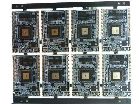
Image 1: GPS Multi-layer PCB
Multilayer PCB In order to increase the area that can be routed, Multilayer PCBs use more single or double-sided wiring boards. With a double-sided inner layer, two single-sided as the outer layer or two double-sided as the inner layer. Two single-sided as the outer layer of the printed circuit board, through the positioning system and insulation bonding materials alternately together and the conductive pattern is interconnected according to the design requirements of the PCB becomes a 4-layer, 6-layer printed circuit board, also known as a multi-layer PCB.
The number of layers of the board does not mean that there are several independent wiring layers, in special cases, empty layers will be added to control the thickness of the board, usually the number of layers is even, and contains the outermost two layers. Most motherboards are 4 to 8 layers, but technically it is possible to achieve nearly 100 layers of PCB boards.
Most of the large supercomputers use quite a few layers of motherboards, but because they can be replaced by clusters of many ordinary computers, super-multilayer PCBs are gradually being used.Because the layers in the PCB are tightly knit, it is generally not easy to see the actual number. But if you look closely at the motherboard, you can still see it.

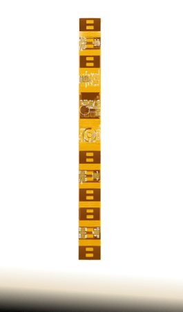
Image 2: Multilayer pcb
Multilayer PCB regardless of its intrinsic quality through the surface. We can see the differences that are critical to the durability and functionality of the PCB throughout its lifetime, the following are the important characteristics of the important high-reliability Multilayer PCB.
Enhanced reliability, including improved z-axis expansion resistance. But there are also certain risks: in the case of practical use, problems with the electrical connection during blowing or degassing, during assembly (separation of inner layers, rupture of the bore wall) or the possibility of failure under load conditions. IPC Class 2 (standard for most factories) requires Multilayer PCBs to be plated with less than 20% copper.
Perfect circuit ensures reliability and safety, no maintenance, no risk. Disadvantages: Multilayer PCB is open if not repaired properly. Even if properly fixed, there may be a risk of failure under load conditions (vibration, etc.), which may lead to failure in actual use.
Improving the cleanliness of Multilayer PCBs improves reliability. Risks: Residues on the terminal block, accumulation of solder can pose a risk of soldering masks, and ionic residues can lead to the risk of corrosion and contamination of the solder surface, which can lead to reliability issues (poor solder points/electrical failures) and ultimately increase the probability of actual failures occurring.

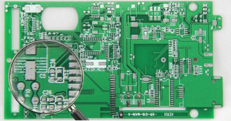
Image 3: The solder mask of multilayer pcb
Soldering, reliability and risk of moisture intrusion Unfinished risk is that the surface treatment of the old Multilayer PCB may lead to metallographic changes, while moisture intrusion may lead to problems in the assembly process and/or the actual use of delamination, separation of inner walls and wall walls (open circuit), etc.
Whether in the manufacturing assembly process or in real-world use, it is critical that Multilayer PCBs perform reliably
Your Trusted Partner for PCB Success: XPCB Limited
Let XPCB Limited be your guide to PCB success. Our comprehensive PCB manufacturing, rapid prototyping, and turnkey PCBA services are designed to meet your needs with ease. Count on us to deliver reliable solutions that exceed your expectations. With XPCB Limited, your journey to PCB excellence starts here.


XPCB Limited is a premium PCB & PCBA manufacturer based in China.
We specialize in multilayer flexible circuits, rigid-flex PCB, HDI PCB, and Rogers PCB.
Quick-turn PCB prototyping is our specialty. Demanding project is our advantage.
Tel : +86-136-3163-3671
Fax : +86-755-2301 2705
Email : [email protected]
© 2024 - XPCB Limited All Right Reserve
