


The structure of PCB board and printed circuit board can generally be divided into two parts, that is, the part of the substrate (generally using engineering plastics with good thermal insulation and insulation, not easy to bend) and the circuit layer-out part, in which the conductive medium used in the layer-out part is copper foil, also called copper skin, which covers the two outer surfaces of the entire base layer.
This layer is the core of the entire PCB. After the designer designs the circuit through various design software, the copper foil layer is engraved by a special machine according to the design drawings. And the unwanted part is carved out, so as to form a complete circuit, and at the same time, various components (chips, resistors, capacitors, inductors, plugs, fuses, etc.) are soldered or patched on the PCB to make it together with the copper foil layer, so as to form a complete circuit.
Usually, the PCB board has two layers, which are located on the upper and lower surfaces of the substrate, and the circuits on the upper and lower layers are different, which is because of the needs of circuit design and safety considerations, such as the lines of the power supply part and the lines of the grounding part, which are generally separated from the circuit layer on the impassable layer.
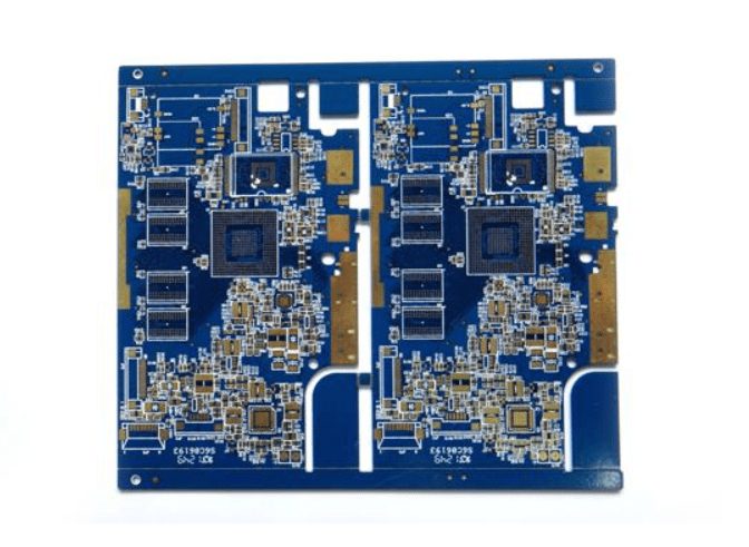
In some special times, for some complex circuits, one layer may not be able to row all the lines or one layer of lines can not realize the control of the circuit (for example, some components have very fine requirements for impedance), then it is necessary to use multi-layer PCB. Multi-layer PCB is actually a single-layer PCB stacked together, so that different circuits can be designed on different circuit layers to meet the needs of complex circuits, and the number of layers of the general PCB is divided into 2 layers, 4 layers, 6 layers, 8 layers, 10 layers, etc.
It is relatively easy to identify whether the PCB circuit board is multi-layered, and you only need to look at the light to observe whether the part that is not covered by copper on the upper and lower surfaces is translucent. Because if there are other circuit layers in between, then the transparency will naturally be low. It is also possible for some senior developers to accurately determine how many layers the PCB is by the naked eye~ But it is difficult to accurately judge how many layers it is.
The substrate material of PCB board
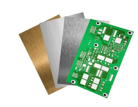
There is no unified standard for the color of the PCB board, so there is no saying that the PCB of other colors must be better than the green one, but in the PCB design, the green plate is the most commonly used, because the green surface does not look dazzling, and some manufacturers in order to highlight their own design, often change the color of the PCB on some relatively high-quality products, such as the PCB of purple ink, the PCB of yellow ink, Black ink PCB and so on to achieve a distinctive visual effect, perhaps this is the source of the feeling that “other colors are better than green”.
First of all, it is according to the customer’s industry needs to stipulate that the PCB is multi layers. For example, a customer is to make the circuit board of the motherboard graphics card, it is only a small part of the purchase. Because all the boards will be tested for reliability before mass production, even if the use of 4-layer boards or even 2-layer boards. It is definitely possible to achieve the requirements of product performance, and because the PCB board has several layers, most businesses will not understand. So this aspect is not of great significance in the actual purchase, and you don’t need to be too restrained.
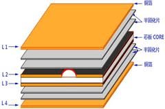
Lamination of PCB board
Make Your PCB Dreams a Reality with XPCB Limited
XPCB Limited is your go-to partner for turning your PCB dreams into reality. Our streamlined PCB manufacturing process, combined with quick-turnaround prototyping and turnkey PCBA services, ensures that your projects come to life with ease. Trust in our expertise and dedication to quality as we help you achieve your PCB goals. Join us and experience the difference with XPCB Limited.
XPCB Limited is a premium PCB & PCBA manufacturer based in China.
We specialize in multilayer flexible circuits, rigid-flex PCB, HDI PCB, and Rogers PCB.
Quick-turn PCB prototyping is our specialty. Demanding project is our advantage.
Tel : +86-136-3163-3671
Fax : +86-755-2301 2705
Email : [email protected]
© 2023 - XPCB Limited All Right Reserve
