


A 6-layer PCB board consists of six layers of conductive material, it consists of a 4-layer PCB board, and two planes between two additional signal layers, a typical 6-layer printed circuit board consists of two inner layers, Two outer layers, and two inner layers, one for power supply and one for grounding, this design can improve electromagnetic interference, provide better routing for low-speed and high-speed signals, double-layer surface helps low-speed signal transmission. Two inner layers help high-speed signal transmission, and the layout of the double-sided panel can be routed is limited, for some products with small volume and high requirements.
The double-sided panel is unable to achieve the line layout effect that customers want, at this time it has to use a 6-layer PCB circuit board to complete. The appropriate stacking of a 6-layer PCB circuit board can improve its performance. Due to the different types of RF equipment, it can effectively control electromagnetic interference and contain multiple isolation components, and any errors in the design will affect the performance of the PCB board. So what should we do when designing the 6-layer PCB circuit board to fully exert the performance of the PCB board to the extreme?
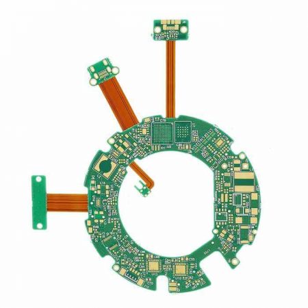
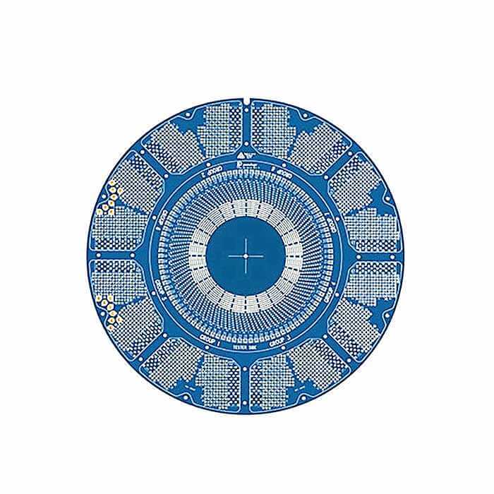
Image 1: Rigid flex 6 layer PCB HDI
The number of ground, power, and signal layers that may be required for the PCB should be analyzed and addressed before designing a 6-layer PCB board, the adhesive layer is an important part of any laminate, providing better shielding for the laminate and reducing the need for an external shielding tank. When planning dense circuit boards with little wiring space, four signal layers can be installed, one ground plane, and one power plane, in a high-density circuit board, wireless and analog signals are mixed.
The signal layer/ground/power plane/ground/signal plane/ground plane separates the internal and external signal layers, this layered design helps in the electromagnetic interference mixing in the internal signal layer, and the stacked design is also ideal for RF equipment, providing decoupling for AC power and ground plane. To build a printed circuit board, there are many sensitive circuits, and choose such a stack: signal/power/2 signal/ground/signal, which can well protect sensitive wiring, and is more suitable for high-frequency analog signals or high-speed digital signal circuits.
These signals will be separated from the low-speed signals on the outer layer, and this shielding is done on the inner layer, which also allows for signal routing at different frequencies or switching speeds. The stacking of ground/signal layer/power/ground/signal layer/ground can be arranged on the circuit board near the strong radiation source, which can effectively control electromagnetic interference, and is also suitable for circuit boards used in noisy environments.
Image 2: 6 layer flexible pcb example
The main principle of the layout is to do a good job of partitioning, that is, the partition of analog devices and digital devices, which can reduce interference. Because the interference generated by digital signals is large and the anti-interference is also strong, while the interference generated by analog signals is relatively small. But it is susceptible to digital signal interference. Another point is to pay attention to the layout of components with different working voltages, and the devices with large voltage differences should be far apart.
For the decoupling capacitors of some chips, the closer to the pins the better. Other things to pay attention to are that the pins of the same network are close together, and pay attention to the aesthetics of the layout. The specific steps of segmentation are as follows:
A. Highlight a certain voltage network, switch to the inner power layer, use line, and draw a closed graph, and the closed area is the network of the voltage;
B. Lead out the pins of the top layer and the ground layer with wires and connect them to the inner power layer through the pads;
C. Draw the next power network, line is the dividing line of the two networks, which is the part that has been corroded.
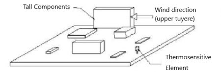
Image 3: Component layout
Attention should be paid to the inner electrical layer: the division distance of the area with large voltage difference should be wide; Unused copper molds can be placed on planes to corrode away areas as they are crafted; Do not place the pad on the split line to affect its contact with the inner electrical layer.
Make Your PCB Dreams a Reality with XPCB Limited
XPCB Limited is your go-to partner for turning your PCB dreams into reality. Our streamlined PCB manufacturing process, combined with quick-turnaround prototyping and turnkey PCBA services, ensures that your projects come to life with ease. Trust in our expertise and dedication to quality as we help you achieve your PCB goals. Join us and experience the difference with XPCB Limited.
XPCB Limited is a premium PCB & PCBA manufacturer based in China.
We specialize in multilayer flexible circuits, rigid-flex PCB, HDI PCB, and Rogers PCB.
Quick-turn PCB prototyping is our specialty. Demanding project is our advantage.
Tel : +86-136-3163-3671
Fax : +86-755-2301 2705
Email : [email protected]
© 2023 - XPCB Limited All Right Reserve
