• +86-755-23012705
  • Building 3, Jinfeng Industrial Park, Fuyong Street, Baoan District, Shenzhen ,China
  • [email protected]
logo
  • Home
  • About Us
    • Flexible PCB Expertise
    • Our Certifications
    • Our Facility
    • Quality Assurance
  • PCB Fabrication
    • Flexible PCB
    • Rigid Flex PCB
    • Rigid PCB
    • ELIC HDI PCB
    • RF PCB
    • Medical PCB
    • Automotive PCB
    • IoT & IIoT PCB
    • Industrial Control PCB
    • Telecommunication PCB
    • Consumer Electronics PCB
  • PCB Assembly
    • Turn Key PCB Assembly
    • Consigned PCB Assembly
    • Components Sourcing
  • Capabilities
    • PCB Fab Capability
    • ATE PCB Fabrication
    • PCB Technology Roadmap
    • PCB Assembly Services
    • PCB Design Support
  • Contact
  • Resources
    • PCB Blog
    • PCB Glossary
Get Quote

Some Precautions In The PCB Production Process 1/2

In the PCB production process, the PCB CAM data generated by CAD must be transmitted to the PCB manufacturer first. The PCB manufacturer uses the CAM 1 data editor to check and edit the film data, hole data, etc.


Add reference marks, correction values required for the production of PCB or data synthesis. For example, check whether the distance between the pad and the aperture is reasonable.


The pads are usually tin-plated, and the plug-in holes are hollow. It can be seen from the PCB design that the pad is ring-shaped.


A few tenths of a millimeter in the PCB design process is all right, but in fact, manufacturers need to have a minimum width standard, and the width design is too small to be produced. On top of the usual design standards, the actual production standards of the PCB manufacturer need to be used to calibrate the design standards.

Some Precautions In The PCB Production Process 1 Some Precautions In The PCB Production Process 1/2

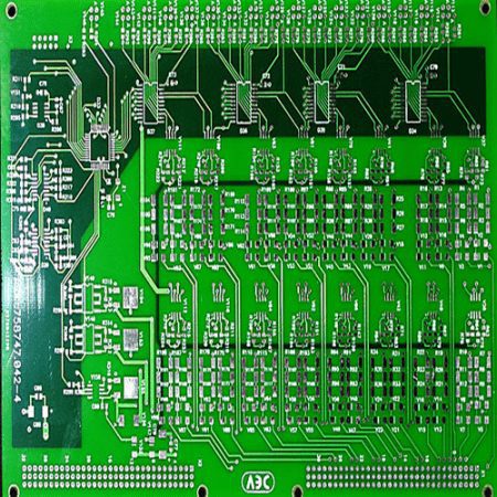
For example, about the minimum width of the pad, some manufacturers can achieve a minimum width of 0.2mm, and some can achieve 0.25mm. If 0.2mm is required, the formation of a pad cannot be guaranteed.


For example 2, check the distance between the window opened on the solder mask and the pad.

Usually, a layer of green film texture on the PCB is the solder mask. That is the solder mask cannot be soldered normally.


The window of the solder mask is usually designed to be larger than the diameter of the pad. This is to maintain a certain distance between the window and the pad.

It is usually set to 0.2mm, so that even if a certain error occurs on the board, the solder mask will not cover the pad, resulting in poor soldering.


Example 3, check the minimum width of traces and the minimum spacing of traces. The usual process can achieve the minimum width and minimum spacing of 0.2mm, respectively. When it is smaller, a special process is required. Only the minimum standards that manufacturers can achieve under normal circumstances are introduced here.


Share

Related posts

dispensing in PCB
2025-02-07

Multilayer PCB Assembly and HDI PCB Manufacturing for High-Tech Solutions


Read more
smt product line
2025-02-06

Streamline Your PCB Production with XPCB’s Turnkey PCBA Services


Read more
2025-02-05

Comprehensive Turnkey PCBA Services: From BOM to SMT Assembly


Read more
amazon
amphenol-logo
halliburton
intel logo
samtec logo
sanmina logo

Company Info

XPCB Limited is a premium PCB & PCBA manufacturer based in China.

We specialize in multilayer flexible circuits, rigid-flex PCB, HDI PCB, and Rogers PCB.

Quick-turn PCB prototyping is our specialty.  Demanding project is our advantage.

Head Office

XPCB Limited
Address :
Building 3, JinFeng Industry Area,  Fuyong Town, Baoan District, Shenzhen, Guangdong, 518103, China.

Tel : +86-136-3163-3671
Fax : +86-755-2301 2705
Email : [email protected]

Quick Links

  • Flexible PCB
  • Rigid Flex PCB
  • ELIC HDI PCB
  • RF PCB
  • PCB Capability
  • PCBA Capabiility
  • About Us

PCB Blog

Multilayer PCB Assembly and HDI PCB Manufacturing for High-Tech Solutions

Read More »

Streamline Your PCB Production with XPCB’s Turnkey PCBA Services

Read More »

Comprehensive Turnkey PCBA Services: From BOM to SMT Assembly

Read More »

© 2024 - XPCB Limited All Right Reserve