


It is apparent that direct chip attaches on PWBs will result in a significant reduction of the packaging efficiency of such assemblies, except for the fact that components can be mounted on both sides of the PWB substrate. It has been shown that wire bonding can be done on both sides of a PWB with some special fixturing; also, outer lead bonding (OLB) of TABs can be done on both sides of the PWB substrate. Thus, while single-sided bare chip assembly on PWBs reduces its packaging efficiency to about half that of other types of substrate constructions, the ability to place components on both sides of PWBs brings it back to the same packaging efficiency level as others.
The continuing increase in component performance and lead PCB density, along with the reduction in package sizes, has required that PWB technology find corresponding ways to increase the interconnection density of the substrate. With the introduction and continued refinement of such packaging techniques as the ball grid array (BGA), chip-scale packaging (CSP), and chip-on-board (COB), traditional PWB technology has approached a point where alternative ways of providing high-density interconnection have had to be developed.
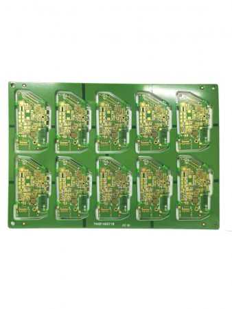
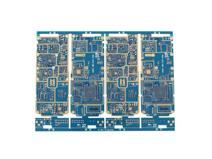
Image 1: 10 Layer HDI rigid flex PCB
This is the most straightforward solution: when there is insufficient room on existing layers to place all the necessary interconnecting paths, add a layer. This approach has been widely practiced in the past, but when the cost-effectiveness of the substrates is of paramount importance, a very careful design analysis must be made to minimize layer counts in MLBs, because there is a significant cost increase with every additional layer in the board. As seen from Calculated for 6- × 8-in MLBs produced in large quantities with yields and conductor density kept constant, there is almost a linear relationship between board costs and layer count.
Any increase in the number of signal layers in boards operating at frequencies requiring transmission line characteristics will double the total number of layers, due to the need to interleave ground or DC power planes between signal planes. There is a definite decrease in the manufacturing yields with an increased number of layers in any of the linewidth categories. This is rather a typical situation in board manufacturing because of increased complexity and thickness of MLB with a higher number of layers usually leads to a larger number of problems on the production floor.
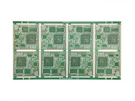
Image 2: HDI pcb manufacturer
There are three basic ways to increase the connectivity or available conductor capacity of PCB density:
Reduce hole and pad diameters,For more information, see the previous blog
Increase the number of conductive channels between pads by reducing the widths of the conductors
Increase the number of signal planes
The effect of each approach on pcb manufacturing yields, and thus onboard costs, will be discussed in sequence. It should be noted that the last option is the simplest but the most costly solution, and thus should be used only after the methods suitable for resolving the first two conditions have been proven inadequate for achieving the desirable board density.
Image 3: 8L high PCB density supplier
Simplify Your PCB Journey with XPCB Limited
XPCB Limited simplifies the PCB process for you. With our quick-turnaround prototyping and turnkey PCBA services, we ensure that your projects move forward smoothly and efficiently. Trust our commitment to quality and timeliness as we help you bring your designs to life. Choose XPCB Limited for a hassle-free PCB experience.
XPCB Limited is a premium PCB & PCBA manufacturer based in China.
We specialize in multilayer flexible circuits, rigid-flex PCB, HDI PCB, and Rogers PCB.
Quick-turn PCB prototyping is our specialty. Demanding project is our advantage.
Tel : +86-136-3163-3671
Fax : +86-755-2301 2705
Email : [email protected]
© 2023 - XPCB Limited All Right Reserve
