


By definition, MLBs have three or more circuit layers. The main applications of MLBs used to be confined to sophisticated industrial electronic products. Now, however, they are the mainstream of all electronic devices, including consumer products such as portable video cameras, cellular phones, and audio discs.
As personal computers and workstations become more powerful, mainframe computers and supercomputers are being replaced in many applications by these smaller machines. As a result, the use of highly sophisticated MLBs, which have layer counts over 70, is being reduced, but the technology to produce them is proven. At the other end of the layer-count spectrum, thin and high-density MLBs with layer counts between 4 and 8 are mainstream. The drive toward thinner MLBs will continue and is made possible by the continuing concurrent advancement of materials and equipment to handle thin core materials.
As PCBs have had to address the issues of higher speed, higher density, and the rise of surface-mount components that use both sides, the need to communicate between layers has increased dramatically. At the same time, the space available for vias has decreased, causing a continuing trend toward smaller holes, more holes on the board, and the decline of the use of holes that penetrate the entire board, which use space on all layers. As a result, the use of buried and blind vias has become a standard part of multilayer board technology, driven by the need for this increased package density.
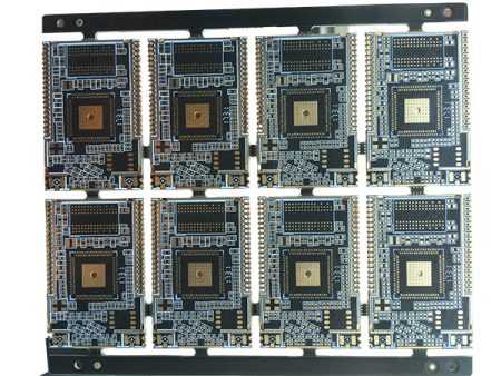
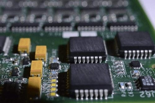
Image 1: GPS Multilayer board Back Drill Hole
One of the immediate issues that arise from these trends is the problems of drilling and the associated cost of this fabrication step. Printed wiring boards, which once were stacked three high on a drilling machine, must be drilled individually, and the number of holes per board has risen, to accommodate the need for vias. This has caused a major problem for fabricators, who
find that a lack of drilling capacity is creating a big demand on funds for additional machines, while the cost of drilling continues to increase dramatically. Therefore, alternate methods for creating vias are being developed. These pressures will be ongoing, and therefore the process listed here, or some equivalent, will undoubtedly become more important as the drive to miniaturization continues and drilling individual holes becomes less and less practical.
Surface Laminar Circuits (SLCs). The most notable MLB technology developed to form vias is the sequential fabrication of multilayers without press operations. This is particularly important for surface blind via holes.
The process for fabricating a board using surface laminar circuits is as follows
Image 2: Multilayer PCBA
A different approach to small via creation has been taken by Dyconex AG of Switzerland. After ground and power patterns are formed on the panel, and the panel is oxide-treated, polyimide-backed copper foil is laminated on the panel. Holes in the copper are formed by a chemical etching process, and the insulating polyimide material underneath the holes is removed by plasma etching. PCBs made in such a way are called DYCOstrate.
In other, similar technologies, different dielectric materials are used, and they are removed by alkaline solutions. The rest of the process is similar to that for SLC; that is, holes are metalized a thick copper deposition is made by electroless or galvanic plating, and the circuit pattern is formed by a tent-and-etch process.
In both SLC and DYCOstrate cases, through-holes can also be made by conventional drilling and plating processes, in addition to the surface blind via holes. Cost Impact. The manufacturing cost of these sequential technologies is not necessarily directly cheaper than conventional MLB technology, which depends on a laminating press operation. However, since the cost of making standard holes in a board can be as high as 30 percent of the total manufacturing cost and the creation of holes in these processes is comparatively inexpensive, the overall cost for equivalent functionality can be less.
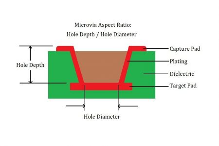
Image 3: Microvia Aspect Ratio
In addition, the fine pattern capability for this process is excellent. For example, an eight-layer conventional structure can often be reduced to a four-layer structure, reducing the total cost of the same packaging density
Discover a World of Possibilities with XPCB Limited
At XPCB Limited, we’re here to help you explore new horizons. Our advanced PCB manufacturing, rapid prototyping, and turnkey PCBA solutions make it easy for you to turn your ideas into reality. Trust us to deliver excellence and reliability every step of the way. Join us and experience the power of innovation with XPCB Limited by your side.
XPCB Limited is a premium PCB & PCBA manufacturer based in China.
We specialize in multilayer flexible circuits, rigid-flex PCB, HDI PCB, and Rogers PCB.
Quick-turn PCB prototyping is our specialty. Demanding project is our advantage.
Tel : +86-136-3163-3671
Fax : +86-755-2301 2705
Email : [email protected]
© 2023 - XPCB Limited All Right Reserve
