• +86-755-23012705
  • Building 3, Jinfeng Industrial Park, Fuyong Street, Baoan District, Shenzhen ,China
  • [email protected]
logo
  • Home
  • About Us
    • Flexible PCB Expertise
    • Our Certifications
    • Our Facility
    • Quality Assurance
  • PCB Fabrication
    • Flexible PCB
    • Rigid Flex PCB
    • Rigid PCB
    • ELIC HDI PCB
    • RF PCB
    • Medical PCB
    • Automotive PCB
    • IoT & IIoT PCB
    • Industrial Control PCB
    • Telecommunication PCB
    • Consumer Electronics PCB
  • PCB Assembly
    • Turn Key PCB Assembly
    • Consigned PCB Assembly
    • Components Sourcing
  • Capabilities
    • PCB Fab Capability
    • ATE PCB Fabrication
    • PCB Technology Roadmap
    • PCB Assembly Services
    • PCB Design Support
  • Contact
  • Resources
    • PCB Blog
    • PCB Glossary
Get Quote

Impact of Blind Via and Buried Via on HDI PCB Performance Optimization

ELIC HDI PCB hdi pcb manufacturer

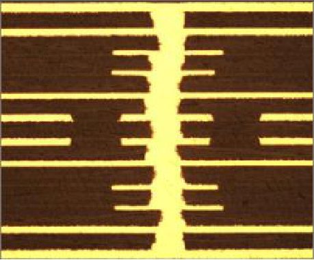
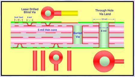
High-Density Interconnect (HDI) PCBs have revolutionized modern electronics, enabling the design of compact, high-performance devices. Among the critical features that distinguish HDI PCBs are blind vias and buried vias. These specialized interconnects play a pivotal role in enhancing the performance, reliability, and manufacturability of HDI PCBs. Understanding their impact is essential for optimizing HDI PCB designs for demanding applications.


Understanding Blind and Buried Vias

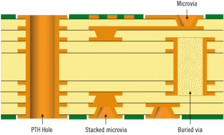
Blind vias are connections that link an outer layer of a PCB to one or more inner layers but do not pass through the entire board. These vias are typically used in HDI designs to save space on densely packed outer layers.

Buried vias, on the other hand, are entirely encapsulated within the inner layers of the PCB and do not extend to the outer layers. These vias are crucial for connecting internal layers without interfering with the surface routing.

Both blind and buried vias enable intricate layer-to-layer connections while maximizing the available surface area for components and traces. This capability is particularly important for HDI PCBs, which are commonly used in mobile devices, wearable electronics, automotive systems, and advanced medical devices.


HDI PCB manufacturer stackup


Impact on Electrical Performance

  1. Signal Integrity: Blind and buried vias reduce parasitic inductance and capacitance compared to through-hole vias. This reduction enhances signal integrity, making these vias ideal for high-speed and high-frequency applications.
  2. Impedance Control: The shorter via length of blind and buried vias minimizes signal reflections and helps maintain controlled impedance. This is crucial for ensuring consistent signal transmission in HDI PCBs used in RF, microwave, and high-speed digital designs.
  3. Crosstalk Reduction: By confining connections within specific layers, buried vias help minimize electromagnetic interference (EMI) and crosstalk between signals, improving overall system performance.


Impact on Thermal Management

  1. Heat Dissipation: In high-power applications, blind and buried vias contribute to effective heat dissipation by providing thermal pathways between layers. This enhances the thermal reliability of the PCB.
  2. Thermal Expansion Management: These vias distribute heat more evenly across the PCB, reducing the risk of warping or delamination caused by uneven thermal expansion.


Impact on Manufacturing and Design Flexibility

  1. Space Optimization: Blind and buried vias free up surface area on the outer layers, allowing for higher component density. This is vital for miniaturized electronics where space is a premium.
  2. Layer Management: These vias enable designers to segregate signal, power, and ground layers more effectively, optimizing the stack-up for performance and manufacturability.
  3. Reduced Drill Count: By limiting the vias to specific layers, the overall drill count and associated costs can be reduced compared to traditional through-hole vias.


HDI PCB stacking BY xpcb


Challenges and Considerations

Despite their advantages, blind and buried vias introduce certain challenges:

  1. Cost: The fabrication of blind and buried vias requires advanced drilling techniques, such as laser drilling, and additional processing steps, which increase manufacturing costs.
  2. Reliability: Ensuring the reliability of these vias is crucial, especially for high-reliability applications. Proper via filling and plating techniques are essential to avoid voids and ensure robust connections.
  3. Design Complexity: Incorporating blind and buried vias demands meticulous design and simulation to optimize the layer stack-up, signal paths, and thermal performance.


Best Practices for Optimization

  1. Use Advanced CAD Tools: Leverage PCB design software with HDI-specific features to effectively plan and simulate via placements and layer stack-ups.
  2. Collaboration with Manufacturers: Engage with PCB manufacturers early in the design process to ensure feasibility and cost-effectiveness of blind and buried vias.
  3. Design for Reliability: Prioritize via reliability by adhering to industry standards and guidelines, such as IPC standards, for via plating and filling.
  4. Thermal Analysis: Conduct thorough thermal simulations to evaluate the impact of vias on heat dissipation and ensure adequate thermal management.


6 layer HDI rigid flex PCB


Conclusion

Blind and buried vias are indispensable tools for optimizing the performance of HDI PCBs. They enable high-density routing, enhance electrical and thermal performance, and support the miniaturization of electronic devices. While they introduce certain challenges, careful design and collaboration with manufacturers can mitigate these issues, unlocking the full potential of HDI PCB technology. By leveraging the advantages of blind and buried vias, engineers can meet the ever-increasing demands of modern electronic applications.


Simplify and Streamline Your PCB Projects with XPCB’s Advanced Manufacturing


Say goodbye to complex PCB processes and hello to simplicity with XPCB Limited. Our advanced PCB manufacturing capabilities allow us to deliver high-quality boards tailored to your unique needs. Whether it’s a simple prototype or a complex multilayer PCB, we streamline the entire process to save you time and resources. Experience effortless PCB manufacturing with XPCB Limited.

Share

Related posts

dispensing in PCB
2025-02-07

Multilayer PCB Assembly and HDI PCB Manufacturing for High-Tech Solutions


Read more
smt product line
2025-02-06

Streamline Your PCB Production with XPCB’s Turnkey PCBA Services


Read more
2025-02-05

Comprehensive Turnkey PCBA Services: From BOM to SMT Assembly


Read more
amazon
amphenol-logo
halliburton
intel logo
samtec logo
sanmina logo

Company Info

XPCB Limited is a premium PCB & PCBA manufacturer based in China.

We specialize in multilayer flexible circuits, rigid-flex PCB, HDI PCB, and Rogers PCB.

Quick-turn PCB prototyping is our specialty.  Demanding project is our advantage.

Head Office

XPCB Limited
Address :
Building 3, JinFeng Industry Area,  Fuyong Town, Baoan District, Shenzhen, Guangdong, 518103, China.

Tel : +86-136-3163-3671
Fax : +86-755-2301 2705
Email : [email protected]

Quick Links

  • Flexible PCB
  • Rigid Flex PCB
  • ELIC HDI PCB
  • RF PCB
  • PCB Capability
  • PCBA Capabiility
  • About Us

PCB Blog

Multilayer PCB Assembly and HDI PCB Manufacturing for High-Tech Solutions

Read More »

Streamline Your PCB Production with XPCB’s Turnkey PCBA Services

Read More »

Comprehensive Turnkey PCBA Services: From BOM to SMT Assembly

Read More »

© 2024 - XPCB Limited All Right Reserve