

The evolution of consumer electronics has been marked by a constant demand for more compact, lightweight, and efficient devices. From smartphones to wearable gadgets, the need for innovation is relentless, driving advancements in printed circuit board (PCB) technology. High-Density Interconnect (HDI) PCBs have emerged as a cornerstone in this domain, enabling the design of smaller, more powerful, and multifunctional electronic devices. A pivotal aspect of HDI PCBs lies in their use of blind vias and buried vias, which contribute significantly to their performance and versatility.
HDI PCBs represent a sophisticated subset of PCB technology characterized by their dense component placement and fine line traces. Unlike traditional PCBs, HDI PCBs use advanced manufacturing techniques to support multiple layers and achieve high interconnectivity within a smaller footprint. The primary features that set HDI PCBs apart include:
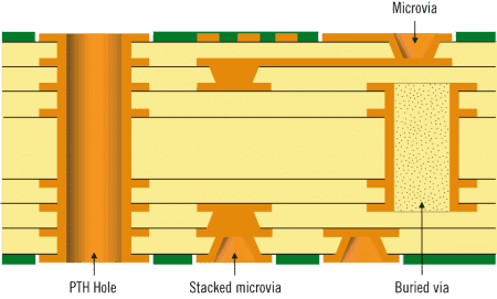
Blind vias and buried vias are integral to the structure and functionality of HDI PCBs. Their inclusion optimizes space utilization, enhances signal integrity, and reduces electrical interference, making them indispensable for consumer electronics.
In consumer electronics, minimizing the size of devices is paramount. Blind and buried vias allow designers to maximize the use of available PCB real estate by enabling multi-layer connections without compromising surface space. This approach ensures that more components can be accommodated within a smaller area, a critical requirement for compact devices like smartphones and tablets.
Signal integrity is a major consideration in PCB design, especially for high-speed applications. Blind and buried vias reduce the length of signal paths, minimizing resistance, capacitance, and inductance effects. This leads to fewer signal losses and improved overall performance. The reduced via stubs also help in mitigating signal reflection and crosstalk, which are common issues in densely populated PCBs.
By keeping interconnects confined within specific layers, blind and buried vias contribute to better control of impedance. This control is essential for maintaining electrical performance, particularly in circuits with high-frequency signals. Additionally, these vias help in efficient power distribution across layers, ensuring reliable device operation.
In high-power applications, effective thermal management is critical to prevent overheating and ensure device longevity. Blind and buried vias facilitate better heat dissipation by providing direct thermal paths between layers. This capability is especially valuable in devices like gaming consoles and advanced computing systems, where heat generation is significant.
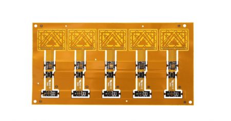
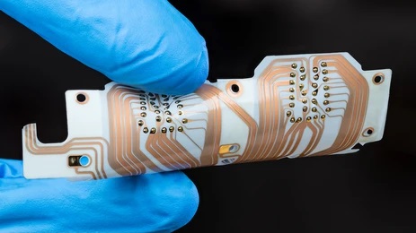
4 layer Flex Circuit with HDI
The use of HDI PCBs with blind and buried vias has revolutionized the design and functionality of consumer electronics. Here are some notable applications:
Modern smartphones rely heavily on HDI PCBs to achieve their slim profiles and high functionality. Blind and buried vias enable multi-layer designs, supporting high-density component placement and complex interconnections. This allows for advanced features like 5G connectivity, high-resolution displays, and enhanced processing power.
Wearable devices, such as fitness trackers and smartwatches, demand ultra-compact PCBs. Blind and buried vias make it possible to integrate multiple features, such as sensors, communication modules, and batteries, within a limited space.
HDI PCBs with blind and buried vias contribute to the sleek and lightweight designs of laptops and tablets. They enable the integration of high-performance processors, memory modules, and graphics units while maintaining device thinness.
Gaming consoles require robust and efficient PCBs to support high-speed data processing and graphics rendering. Blind and buried vias enhance signal integrity and thermal management, ensuring smooth performance even during extended gaming sessions.
The Internet of Things (IoT) ecosystem depends on miniaturized, efficient electronics. HDI PCBs with blind and buried vias enable the design of compact and reliable IoT devices, ranging from smart home systems to industrial sensors.
The adoption of blind and buried vias in HDI PCBs offers several advantages:
Despite their advantages, the implementation of blind and buried vias poses certain challenges:
The application of HDI PCBs in consumer electronics has transformed the industry, enabling the production of innovative, compact, and high-performance devices. Blind and buried vias play a crucial role in this transformation, providing the means to achieve space optimization, enhanced signal integrity, and superior electrical performance. As consumer electronics continue to evolve, the adoption of HDI PCBs and their advanced features will remain pivotal in meeting the demands of a technology-driven world. By overcoming the associated challenges, manufacturers can leverage the full potential of HDI PCBs to push the boundaries of what’s possible in consumer electronics.
Simplify and Streamline Your PCB Projects with XPCB’s Advanced Manufacturing
Say goodbye to complex PCB processes and hello to simplicity with XPCB Limited. Our advanced PCB manufacturing capabilities allow us to deliver high-quality boards tailored to your unique needs. Whether it’s a simple prototype or a complex multilayer PCB, we streamline the entire process to save you time and resources. Experience effortless PCB manufacturing with XPCB Limited.
XPCB Limited is a premium PCB & PCBA manufacturer based in China.
We specialize in multilayer flexible circuits, rigid-flex PCB, HDI PCB, and Rogers PCB.
Quick-turn PCB prototyping is our specialty. Demanding project is our advantage.
Tel : +86-136-3163-3671
Fax : +86-755-2301 2705
Email : [email protected]
© 2024 - XPCB Limited All Right Reserve
