

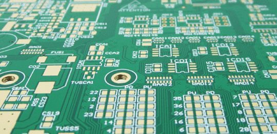
 Is there any difference between PCB gold plating and immersion gold
At the time of early PCB processing, surface treatment of tin USES the most widespread, it has excellent welding performance and low cost, and with the refinement of PCB, tin process is difficult to tiny solder leveling, this brought difficulty to SMT, and short service life of the tin plate, the gold look good solve these problems.
When it comes to gold boards, PCB manufacturers will ask you whether to make ENIG or gold, soft gold or hard gold, which can be confusing for PCB designers. Today we will talk about different gold boards:
According to the different processing technology is divided into: electric gold plating, chemical gold sink.
Electric Gold plating: with electrolytic principle, a thin layer of Gold is plated on nickel. It has strong corrosion resistance, good electrical conductivity, easy welding, high temperature resistance, corrosion resistance and wear resistance to some extent.
According to the purity of gold, electric gold plating is divided into soft gold and hard gold:
Soft gold: Pure gold is called soft gold because of its high purity.
Hard gold: To increase the hardness of the surface, other metals are added called hard gold.
Chemical gold deposition is a process of thin gold deposition through controlled REDOX reaction under the catalytic action of metals. The method of chemical replacement is used to produce the effect of the surface gold layer, so the maximum thickness of the gold layer in principle cannot reach the same thickness as electric gold plating, and the lower the gold content will be less, the thickness is generally 1-3 micro inches.
Process of PCB ENIG:
Whole hole – degreasing – washing – micro-etching – washing – activation – washing – nickel – washing – gold – washing – drying.
The entire hole: The remaining palladium in the non-conducting hole is inactivated by hydrochloric acid or thiourea to prevent it from settling into nickel gold.
Oil removal: Use acid oil remover to remove light grease and oxide from copper surface to clean and increase wettability.
Washing: Reverse flow washing after removing the oil cylinder.
Microetching: Acid sodium persulfate corrosion solution is used to make the copper surface slightly coarse and increase the precision of copper and chemical nickel layer.
Activation: In the electrochemical sequence, copper is located behind nickel, so the copper surface must be activated before electroless nickel plating can be carried out. In the PCB industry, a replacement palladium layer is mostly produced on the copper surface to activate it. The activator is generally sulfuric acid type and hydrochloric acid type, and palladium sulfate is more often used to activate the night, the effect is more ideal.
Nickel deposition: Nickel ions deposited on bare copper surfaces under the condition of sodium hypophosphate reduction under the activation of palladium. When nickel is deposited over the palladium-catalyzed crystal, the autocatalytic reaction continues until the desired nickel thickness is obtained.
Immersion gold: After the nickel layer on the PCB surface is put into the gold tank, the nickel surface is attacked by the tank solution and the nickel ions are dissolved. The two electrons are obtained by the gold cyanide ions and the gold layer is deposited on the nickel surface.
PCB gilt plate because of its excellent electrical conductivity, wear resistance and oxidation resistance are often used in gold finger plate and bond plate. The gold layer on a PCB as a metal corrosion resistant layer can withstand all general etching solution. It has a very high conductivity. Due to its negative oxidation potential, it is an ideal corrosion resistant metal.
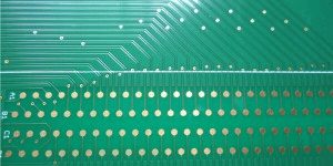
Printed circuit boards are usually plated with hard gold to provide contact points and PCB edge connectors.
Gold contact surfaces are commonly used on circuit boards. Thin-film switches are the preferred technology for industrial, commercial and consumer products. When the PCB is repeatedly installed and removed, electric gold plating is used for edge connector contacts or, more commonly, gold fingers. In the 1964 James Bond film, it’s hard to hear the word goldfinger without remembering the villain Golden finger. However, the goldfinger (gold-plated stylus) found on the PCB is quite different from the short, chunky Auric number. First, the coating on a PCB goldfinger is usually only 30 microinches thick. At this thickness, hard gold is expected to survive 1,000 cycles before it wears out.
On the Omni circuit board, we have the internal capability to produce the hard gilding required for the contacts and the goldfinger.
After copper etching and PCBs band lamination, the process begins, leaving only the required areas exposed. Electroplate the bottom layer of nickel onto the PCB with a minimum thickness of 50 micro inches. Nickel provides not only mechanical support but also a diffusion barrier as well as pore and creep corrosion inhibitors. A 24-carat hard gold immersed in salt is then plated directly onto the nickel surface.
Quality control of hard gold finishes includes thickness and tape adhesion tests. As you might expect, gold prices require solid process control, as the cost of errors can even make Auric shiver. The calculation of determining the amount of gold required is a function of plating time.
A simple calculator is provided below to determine the approximate weight of the gold consumed by the edge connector. Simply provide the size (in inches) of the gold and multiply the resulting weight by the current price (the LME is a good resource).
The Goldfinger/edge connector requires some design rules.
■ Through-hole plating is not allowed in the plating area
■ There should be no welding mask or screen printing in the electroplating area
■ For panelling, always place the goldfinger outwards from the center of the panel
■ Connect all goldfingers, using 0.008 “conductor trail line allowed to make edge
■ Features can be placed on one or both sides to a depth of 25mm from the outer edge
The ability to provide 24 carat hard gold PCB plating internally not only ensures that we have control over the process, but it also significantly reduces the manufacturing cycle time for fast switching PCBS compared to subcontracting or outsourcing.
XPCB Limited is a premium PCB & PCBA manufacturer based in China.
We specialize in multilayer flexible circuits, rigid-flex PCB, HDI PCB, and Rogers PCB.
Quick-turn PCB prototyping is our specialty. Demanding project is our advantage.
Tel : +86-136-3163-3671
Fax : +86-755-2301 2705
Email : [email protected]
© 2023 - XPCB Limited All Right Reserve
