


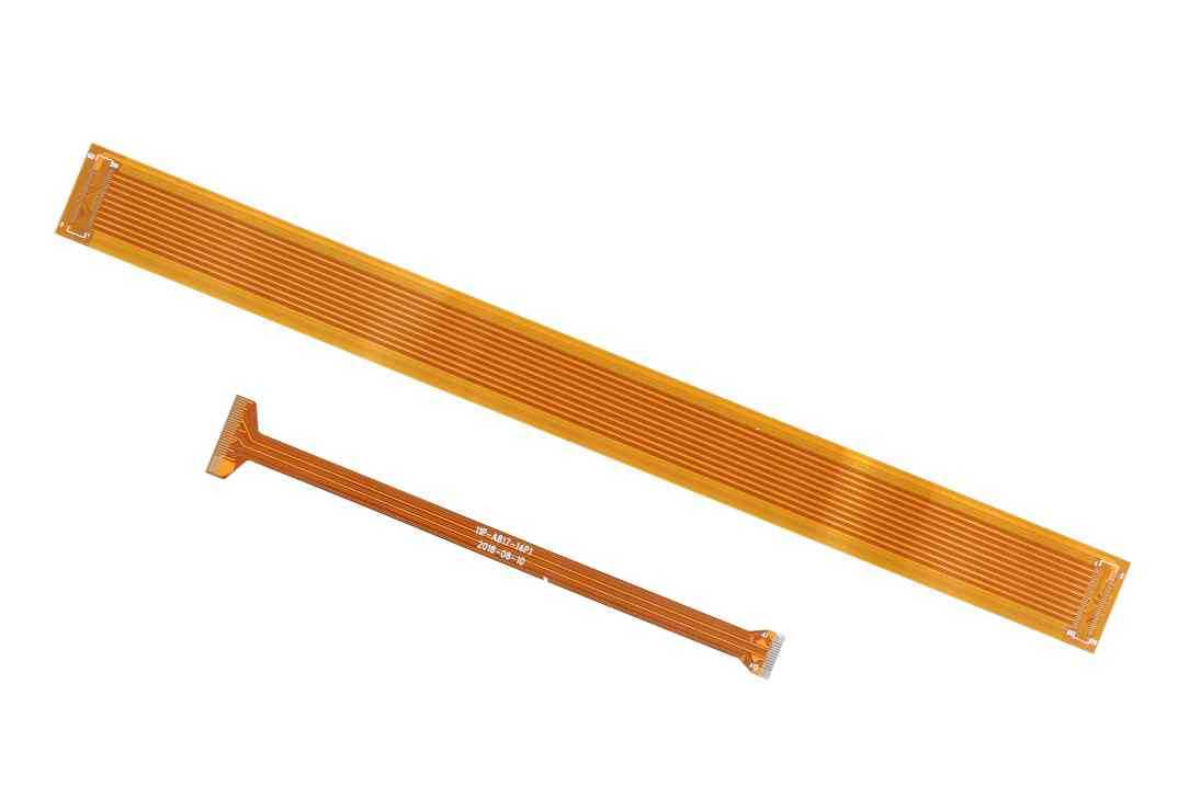
Following previous part 1, here are more design tips on the flexible circuit design guide.
Due to the particularity of FPC, the following points need to be paid attention to when wiring:
Wiring rules: Prioritize the signal wiring to be smooth, follow the principle of short, straight, and less perforation, try to avoid long, thin, and circle wiring, mainly horizontal, vertical, and 45-degree lines, avoid random The angle line and the curved part follow the arc line. The above conditions are described in detail as follows:
1. Line width: Considering that the line width requirements of the data line and the power line are inconsistent, the reserved wiring space is 0.15mm on average
2. Line pitch: According to the current production capacity of most manufacturers, the design line pitch (Pitch) is 0.10mm
3. Line margin: The distance between the outermost line and the FPC contour is designed to be 0.30mm, and the larger the space is, the better
4. Internal fillet: The minimum internal fillet on the FPC profile is designed to be radius R=1.5mm
5. The wire is perpendicular to the bending direction
6. The wire should pass through the bending area evenly
7. The wire should be as full as possible in the bending area
8. There should be no additional plating metal in the bending area (the wires in the bending area are not plated)
9. Keep the line width the same
10. The traces of the double panels cannot overlap to form an “I” shape
11. Minimize the number of layers in the bending area
12. There should be no vias and metalized holes in the bending area
13. The bending center axis should be set at the center of the wire. The material coefficient and thickness on both sides of the wire should be as consistent as possible. This is very important in dynamic bending applications.
14. The horizontal plane torsion follows the following principles-reduce the bending section to increase flexibility, or partly increase the area of copper foil to increase toughness.
15. For vertical bending, increase the bending radius and reduce the number of layers in the central area of the bending.
16. For products with EMI requirements, if high-frequency radiation signal lines such as USB, MIPI, etc. are on the FPC, a conductive silver foil layer should be added to the FPC according to the EMI measurement situation and the conductive silver foil should be grounded to prevent EMI.
XPCB Limited is a premium PCB & PCBA manufacturer based in China.
We specialize in multilayer flexible circuits, rigid-flex PCB, HDI PCB, and Rogers PCB.
Quick-turn PCB prototyping is our specialty. Demanding project is our advantage.
Tel : +86-136-3163-3671
Fax : +86-755-2301 2705
Email : [email protected]
© 2023 - XPCB Limited All Right Reserve
