• +86-755-23012705
  • Building 3, Jinfeng Industrial Park, Fuyong Street, Baoan District, Shenzhen ,China
  • [email protected]
logo
  • Home
  • About Us
    • Flexible PCB Fabrication
    • PCB Fab Capability
    • Our Certifications
    • Our Facility
    • Quality Assurance
  • PCB Fabrication
    • Flexible PCB
    • Rigid Flex PCB
    • Rigid PCB
    • ELIC HDI PCB
    • RF PCB
    • Medical PCB
    • Automotive PCB
    • IoT & IIoT PCB
    • Industrial Control PCB
    • Telecommunication PCB
    • Consumer Electronics PCB
  • PCB Assembly
    • Turn Key PCB Assembly
    • Consigned PCB Assembly
    • Components Sourcing
  • Resources
    • PCB Glossary
    • PCB Design Guide
    • PCB Blog
  • Contact
  • Home
  • About Us
    • Flexible PCB Fabrication
    • PCB Fab Capability
    • Our Certifications
    • Our Facility
    • Quality Assurance
  • PCB Fabrication
    • Flexible PCB
    • Rigid Flex PCB
    • Rigid PCB
    • ELIC HDI PCB
    • RF PCB
    • Medical PCB
    • Automotive PCB
    • IoT & IIoT PCB
    • Industrial Control PCB
    • Telecommunication PCB
    • Consumer Electronics PCB
  • PCB Assembly
    • Turn Key PCB Assembly
    • Consigned PCB Assembly
    • Components Sourcing
  • Resources
    • PCB Glossary
    • PCB Design Guide
    • PCB Blog
  • Contact
Get Instant Quote

What Are the Disadvantages of PCB Surface Treatment Process?

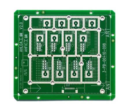
Any PCB circuit board will be accompanied by a detailed description of the PCB surface treatment process. The choice of PCB surface treatment process has a direct impact on the product quotation. Of course, different process treatments have their advantages and disadvantages. The most important thing depends on where the product is applied. Let’s take a look at the common defects of PCB surface treatment process:

1. OSP Organic Anti-Oxidation:

It is very simply affected by acid and humidity. PCB storage time exceeds 3 months and needs to be re-surfaced processing treatment, used within 24 hours after opening the package. OSP is an insulating layer. It is sometimes necessary to print solder paste to process the original OSP layer at the test point before touching the pins for electrical testing.


2. Hot Air Leveling:

Pins with fine gaps and tiny components are not suitable for soldering. Because the PCB spray tin plate has poor surface flatness, and tin beads are prone to appear during PCB processing. It is easy to form a short circuit.


3. Chemically Immersed Silver:

Not only the cost is high when making PCB boards, but the welding performance is also not very good. Using the electroless nickel process, the black plate can be easily formed, and the nickel layer will also be oxidized constantly. Long-term reliability is also a problem.


4. Electroplating of Nickel Gold:

PCB board processed by electroplating of nickel gold, the color is slightly inferior to immersion gold. It is not as bright as other processes.
6.1 What Are the Disadvantages of PCB Surface Treatment Process?

As a printed circuit board manufacturer with our own factory, XPCB Limited has been committed to providing electronic partners with the best PCB products and services. After 16 years of development, XPCB Limited has established a good reputation in the local PCB industry, and will continue to improve production efficiency, reduce costs, bring cost-effectiveness to partners, and maintain high standards of quality and solutions to meet customer requirements.

 

Share

Related posts

Gold finger PCB
2024-04-13

What Is The Difference Between PCB Immersion Gold And Gold Plating


Read more
China quick-turn rigid flex PCB manufacturer
2024-04-12

Do You Know Rapid Flex PCB Have 5 Benefits?


Read more
PCB design guidelines
2024-04-11

About PCB Diagram Design To 5 Frequently Questions


Read more
amazon
amphenol-logo
halliburton
intel logo
samtec logo
sanmina logo

Company Info

XPCB Limited is a premium PCB & PCBA manufacturer based in China.

We specialize in multilayer flexible circuits, rigid-flex PCB, HDI PCB, and Rogers PCB.

Quick-turn PCB prototyping is our specialty.  Demanding project is our advantage.

Head Office

XPCB Limited
Address :
Building 3, JinFeng Industry Area,  Fuyong Town, Baoan District, Shenzhen, Guangdong, 518103, China.

Tel : +86-136-3163-3671
Fax : +86-755-2301 2705
Email : [email protected]

Quick Links

  • Flexible PCB
  • Rigid Flex PCB
  • ELIC HDI PCB
  • RF PCB
  • PCB Capability
  • PCBA Capabiility
  • About Us

PCB Blog

What Is The Difference Between PCB Immersion Gold And Gold Plating

Read More »

Do You Know Rapid Flex PCB Have 5 Benefits?

Read More »

About PCB Diagram Design To 5 Frequently Questions

Read More »

© 2023 - XPCB Limited All Right Reserve