


Multi-layer PCBs are used as the “core force” in the fields of communications, medical treatment, industrial control, security, automobiles, electric power, aviation, military industry, and computer peripherals. Product functions are getting higher and higher, and PCBs are getting more and more sophisticated, so relative to the difficulty of production also getting bigger.
1. Difficulties in Making Inner Circuit
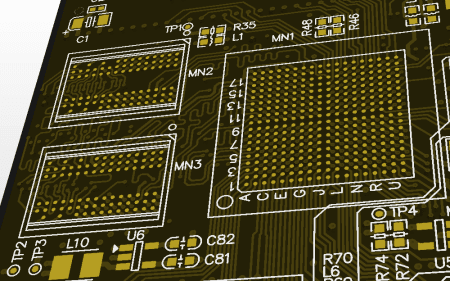
The multilayer circuit has various special requirements for high speed, thick copper, high frequency, and high Tg value. The requirements for inner layer wiring and pattern size control are getting higher and higher. For example, the ARM development board has a lot of impedance signal lines in the inner layer. To ensure the integrity of the impedance increases the difficulty of the inner line production.
There are many signal lines in the inner layer, and the width and spacing of the lines are basically about 4mil or less. The thin production of multi-core boards is prone to wrinkles, and these factors will increase the production of the inner layer.
Suggestion: Design the line width and line spacing above 3.5/3.5mil (most factories have no difficulty in production).
For example, for a six-layer board, it is recommended to use a fake eight-layer structure design, which can meet the impedance requirements of 50ohm, 90ohm, and 100ohm with a 4-6mil line width in the inner layer.
2. Difficulties in Alignment Between Inner Layers
The number of multi-layer boards is increasing, and the alignment requirements of the inner layers are getting higher and higher. The film will expand and contract due to the influence of the temperature and humidity of the workshop environment, and the core board will have the same expansion and contraction when produced, which makes it more difficult to control the alignment accuracy between the inner layers.
3. Difficulties in the Pressing Process
The superposition of multiple core plates and PP (cured plate) is prone to problems such as delamination, sliding plate and steam drum residue during pressing. In the structural design process of the inner layer, factors such as the dielectric thickness between the layers, the glue flow, and the heat resistance of the sheet should be considered, and the corresponding laminated structure should be reasonably designed.
Recommendation: Keep the inner layer of copper spread evenly, and spread the copper in a large area without the same area with the same balance as PAD.
4. Difficulties in Drilling Production
The multi-layer board uses high Tg or other special plates, and the roughness of the drilling of different materials is different, which increases the difficulty of removing the slag in the hole. High-density multi-layer boards have high hole density and low production efficiency, which is easy to break. Between the via holes of different networks, the edge of the hole is too close to cause the CAF effect problem.
Suggestion: The hole edge spacing of different networks is ≥0.3mm.
XPCB Limited is a premium PCB & PCBA manufacturer based in China.
We specialize in multilayer flexible circuits, rigid-flex PCB, HDI PCB, and Rogers PCB.
Quick-turn PCB prototyping is our specialty. Demanding project is our advantage.
Tel : +86-136-3163-3671
Fax : +86-755-2301 2705
Email : [email protected]
© 2023 - XPCB Limited All Right Reserve
