• +86-755-23012705
  • [email protected]
  • Building 3, Jinfeng Industrial Park, Fuyong Street, Baoan District, Shenzhen ,China
Search
Close
logo
  • Home
  • About Us
    • About XPCB
    • Flexible PCB Fabrication
    • PCB Fab Capability
    • PCBA Capability
    • Our Certifications
    • Our Facility
    • Quality Assurance
  • PCB Fabrication
    • Flexible PCB
    • Rigid Flex PCB
    • Rigid PCB
    • ELIC HDI PCB
    • RF PCB
    • Medical PCB
    • Automotive PCB
    • IoT & IIoT PCB
    • Industrial Control PCB
    • Telecommunication PCB
    • Consumer Electronics PCB
  • PCB Assembly
    • Turn Key PCB Assembly
    • Consigned PCB Assembly
    • Components Sourcing
  • Resources
    • PCB Glossary
    • PCB Design Guide
    • PCB Blog
  • Contact
Menu
  • Home
  • About Us
    • About XPCB
    • Flexible PCB Fabrication
    • PCB Fab Capability
    • PCBA Capability
    • Our Certifications
    • Our Facility
    • Quality Assurance
  • PCB Fabrication
    • Flexible PCB
    • Rigid Flex PCB
    • Rigid PCB
    • ELIC HDI PCB
    • RF PCB
    • Medical PCB
    • Automotive PCB
    • IoT & IIoT PCB
    • Industrial Control PCB
    • Telecommunication PCB
    • Consumer Electronics PCB
  • PCB Assembly
    • Turn Key PCB Assembly
    • Consigned PCB Assembly
    • Components Sourcing
  • Resources
    • PCB Glossary
    • PCB Design Guide
    • PCB Blog
  • Contact
Get Instant Quote

Analysis of the Bad Problem of Voids on SMT Patch Processing

In our previous analysis, the voids are already familiar to us, especially the void rate that exceeds the reliability expectations. Special attention should be paid to related problems and possible adverse consequences.

Void is not an absolute bad thing. The related welding quality problems in PCBA process will not even enter the top 5. Moreover, the voids caused by the shrinkage caused by the solidification of the solder are not directly processed by the chip processing plant, and are due to the selection of unreasonable solder paste.

Analysis of the Bad Problem of Voids on SMT Patch Processing Analysis of the Bad Problem of Voids on SMT Patch Processing

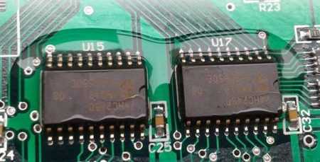
So let’s share with you the other problems caused by the void in the SMT process below:

1. Shrinkage Void: It is formed by the solidification and shrinkage of solder. Most SAC solders and other lead-free solders generally shrink when solidified. Such voids generally do not appear at the interface between the PCB and the pad, and will not affect reliability (there is no possibility of cracks extending to the interface between the solder and the PCB)

2. Microvia Void: Appears on the PCB pad microvia. If this design is located in a solder joint with relatively high stress, it will have an impact on reliability. Generally, it can be solved by electric filling in the blanks.

3. MC Microvoid: It is easy to appear between Cu and high alloy. Generally, it does not appear immediately after welding. The reason for occurrence during high temperature or high temperature cycle is not very clear. It has an impact on the screenability.

Share

Related posts

2022-05-20

Electromagnetic Compatibility Design of Mobile Phone PCB (1)


Read more
2022-05-20

The PCB Circuit Design of LED Switching Power Supply


Read more
2022-05-20

Electromagnetic Compatibility Design of Mobile Phone PCB (2)


Read more
amazon
amphenol-logo
halliburton
intel logo
samtec logo
sanmina logo
Previous
Next

Company Info

XPCB Limited is a premium PCB & PCBA manufacturer based in China.

We specialize in multilayer flexible circuits, rigid-flex PCB, HDI PCB, and Rogers PCB.

Quick-turn PCB prototyping is our specialty.  Demanding project is our advantage.

Head Office

XPCB Limited
Address :
Building 3, JinFeng Industry Area,  Fuyong Town, Baoan District, Shenzhen, Guangdong, 518103, China.

Tel : +86-136-3163-3671
Fax : +86-755-2301 2705
Email : [email protected]

Quick Links

  • Flexible PCB
  • Rigid Flex PCB
  • ELIC HDI PCB
  • RF PCB
  • PCB Capability
  • PCBA Capabiility
  • About Us

PCB Blog

Electromagnetic Compatibility Design of Mobile Phone PCB (1)

Read More »

The PCB Circuit Design of LED Switching Power Supply

Read More »

Electromagnetic Compatibility Design of Mobile Phone PCB (2)

Read More »

© 2023 - XPCB Limited All Right Reserve