• +86-755-23012705
  • [email protected]
  • Building 3, Jinfeng Industrial Park, Fuyong Street, Baoan District, Shenzhen ,China
Search
Close
logo
  • Home
  • About Us
    • About XPCB
    • Flexible PCB Fabrication
    • PCB Fab Capability
    • PCBA Capability
    • Our Certifications
    • Our Facility
    • Quality Assurance
  • PCB Fabrication
    • Flexible PCB
    • Rigid Flex PCB
    • Rigid PCB
    • ELIC HDI PCB
    • RF PCB
    • Medical PCB
    • Automotive PCB
    • IoT & IIoT PCB
    • Industrial Control PCB
    • Telecommunication PCB
    • Consumer Electronics PCB
  • PCB Assembly
    • Turn Key PCB Assembly
    • Consigned PCB Assembly
    • Components Sourcing
  • Resources
    • PCB Glossary
    • PCB Design Guide
    • PCB Blog
  • Contact
Menu
  • Home
  • About Us
    • About XPCB
    • Flexible PCB Fabrication
    • PCB Fab Capability
    • PCBA Capability
    • Our Certifications
    • Our Facility
    • Quality Assurance
  • PCB Fabrication
    • Flexible PCB
    • Rigid Flex PCB
    • Rigid PCB
    • ELIC HDI PCB
    • RF PCB
    • Medical PCB
    • Automotive PCB
    • IoT & IIoT PCB
    • Industrial Control PCB
    • Telecommunication PCB
    • Consumer Electronics PCB
  • PCB Assembly
    • Turn Key PCB Assembly
    • Consigned PCB Assembly
    • Components Sourcing
  • Resources
    • PCB Glossary
    • PCB Design Guide
    • PCB Blog
  • Contact
Get Instant Quote

Analyze the Causes and Solutions of Poor PCB Surface Mount Soldering

1. Bridging

The causes of bridging are mostly caused by excessive solder or severe edge collapse after solder printing, or the size of PCB substrate solder area is out of tolerance, SMD placement offset, etc., when SOP and QFP circuits tend to be miniaturized, bridging will cause an electrical short circuit and affect the use of the product.

Analyze the Causes and Solutions of Poor PCB Surface Mount Soldering Analyze the Causes and Solutions of Poor PCB Surface Mount Soldering

2. Poor Wetting

Poor wetting refers to the fact that the solder and PCB substrate welding area during the soldering process does not generate metal-to-metal reaction after wetting, which results in missing soldering or fewer soldering failures. The reason is mostly caused by contamination of the surface of the soldering zone, or solder resist, or a metal compound layer formed on the surface of the joined object. For example, if there are sulfides on the surface of silver and oxides on the surface of tin, poor wetting will occur. In addition, when the residual aluminum, zinc, cadmium, etc. in the solder exceeds 0.005%, the degree of activity is reduced due to the moisture absorption of the flux, and poor wetting may also occur. In wave soldering, if there is gas on the surface of the PCB substrate, this failure is also prone to occur. Therefore, in addition to performing a proper soldering process, anti-fouling measures must be taken for the surface of the PCB substrate and the surface of the components, selecting the appropriate solder, and setting a reasonable soldering temperature and time.

Share

Related posts

2022-05-20

Electromagnetic Compatibility Design of Mobile Phone PCB (1)


Read more
2022-05-20

The PCB Circuit Design of LED Switching Power Supply


Read more
2022-05-20

Electromagnetic Compatibility Design of Mobile Phone PCB (2)


Read more
amazon
amphenol-logo
halliburton
intel logo
samtec logo
sanmina logo
Previous
Next

Company Info

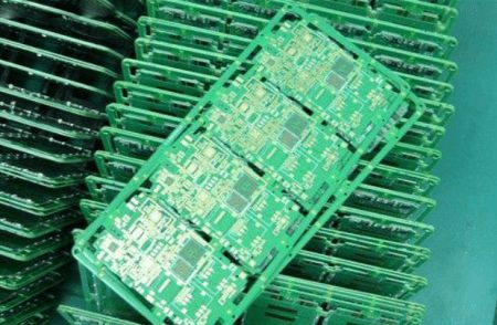
XPCB Limited is a premium PCB & PCBA manufacturer based in China.

We specialize in multilayer flexible circuits, rigid-flex PCB, HDI PCB, and Rogers PCB.

Quick-turn PCB prototyping is our specialty.  Demanding project is our advantage.

Head Office

XPCB Limited
Address :
Building 3, JinFeng Industry Area,  Fuyong Town, Baoan District, Shenzhen, Guangdong, 518103, China.

Tel : +86-136-3163-3671
Fax : +86-755-2301 2705
Email : [email protected]

Quick Links

  • Flexible PCB
  • Rigid Flex PCB
  • ELIC HDI PCB
  • RF PCB
  • PCB Capability
  • PCBA Capabiility
  • About Us

PCB Blog

Electromagnetic Compatibility Design of Mobile Phone PCB (1)

Read More »

The PCB Circuit Design of LED Switching Power Supply

Read More »

Electromagnetic Compatibility Design of Mobile Phone PCB (2)

Read More »

© 2023 - XPCB Limited All Right Reserve