• +86-755-23012705
  • Building 3, Jinfeng Industrial Park, Fuyong Street, Baoan District, Shenzhen ,China
  • [email protected]
logo
  • Home
  • About Us
    • Flexible PCB Expertise
    • Our Certifications
    • Our Facility
    • Quality Assurance
  • PCB Fabrication
    • Flexible PCB
    • Rigid Flex PCB
    • Rigid PCB
    • ELIC HDI PCB
    • RF PCB
    • Medical PCB
    • Automotive PCB
    • IoT & IIoT PCB
    • Industrial Control PCB
    • Telecommunication PCB
    • Consumer Electronics PCB
  • PCB Assembly
    • Turn Key PCB Assembly
    • Consigned PCB Assembly
    • Components Sourcing
  • Capabilities
    • PCB Fab Capability
    • ATE PCB Fabrication
    • PCB Technology Roadmap
    • PCB Assembly Services
    • PCB Design Support
  • Contact
  • Resources
    • PCB Blog
    • PCB Glossary
Get Quote

Application of HDI Technology and Blind Via/Buried Via Integration in Complex PCB Manufacturing

HDI Rigid PCB factory

High-Density Interconnect (HDI) technology has become a cornerstone of modern printed circuit board (PCB) manufacturing. With the rise in demand for compact, high-performance electronics, the integration of HDI technology, combined with blind-via and buried-via designs, plays a pivotal role in enabling advanced, complex PCB architectures. This article delves into the applications and advantages of these technologies in complex PCB manufacturing, shedding light on their transformative impact.


Understanding HDI Technology

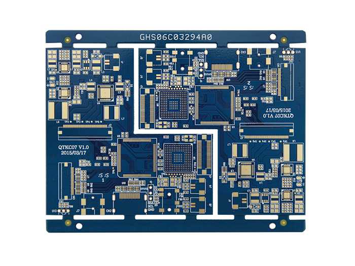
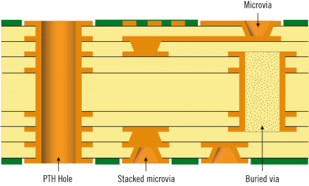
HDI PCBs are characterized by their higher wiring density per unit area compared to traditional PCBs. They achieve this by utilizing smaller vias, finer lines and spaces, and more precise component placement. HDI technology supports advanced features like:

  • Microvias: Tiny vias that connect layers directly, often with a diameter less than 150 µm.
  • Blind Vias: Vias that start on one layer but do not extend through the entire board.
  • Buried Vias: Vias confined entirely within the internal layers of the PCB.

These design elements allow for a reduction in board size while maintaining or even increasing functionality, making HDI an essential choice for miniaturized devices like smartphones, wearables, and IoT devices.


The Role of Blind and Buried Vias

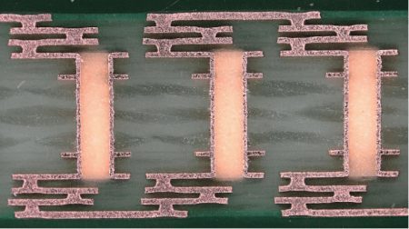
Blind and buried vias are critical in achieving the compactness and high functionality of HDI PCBs. Their unique configurations offer several advantages:

  1. Space Optimization: Blind vias connect the outer layers to inner layers without passing through the entire PCB, saving valuable surface space for component placement. Similarly, buried vias interconnect internal layers without interfering with outer-layer designs.
  2. Improved Signal Integrity: By minimizing via length, blind and buried vias reduce parasitic inductance and capacitance, enhancing signal performance in high-frequency applications.
  3. Enhanced Layer Interconnectivity: These vias enable complex multilayer designs, supporting the intricate routing required in advanced electronic devices.
  4. Thermal Management: Strategic via placement improves heat dissipation, ensuring reliability in high-power applications.


HDI stackup


Applications of HDI Technology in Complex PCB Manufacturing

The integration of HDI technology and blind/buried vias unlocks numerous possibilities in complex PCB manufacturing. Key applications include:

  1. Consumer Electronics:
    • Smartphones and Tablets: HDI PCBs enable compact designs with enhanced functionality, accommodating high-speed processors, memory chips, and antennas within limited space.
    • Wearables: Devices like smartwatches benefit from HDI’s ability to integrate numerous features into a lightweight, small form factor.
  2. Automotive Electronics:
    • Advanced driver-assistance systems (ADAS) and infotainment systems rely on HDI PCBs for high-speed data transmission and compact designs.
    • Blind and buried vias enhance reliability in harsh automotive environments by reducing mechanical stress.
  3. Medical Devices:
    • Devices such as pacemakers, hearing aids, and diagnostic tools leverage HDI PCBs for their miniaturization and reliability.
    • High-density interconnections ensure precise functionality in life-critical applications.
  4. Networking and Telecommunications:
    • High-performance routers and switches require HDI PCBs for high-speed data handling and signal integrity.
    • Blind and buried vias support the multilayer architectures necessary for advanced communication protocols.


Advantages of HDI with Blind and Buried Vias in Manufacturing

When implemented effectively, HDI technology with blind and buried vias offers several manufacturing advantages:

  1. Size and Weight Reduction: Ideal for applications requiring lightweight, compact devices.
  2. Improved Electrical Performance: Shorter signal paths and reduced parasitic effects enhance performance.
  3. Cost Efficiency: Though initially more expensive, the ability to integrate more functionality into a smaller space can reduce overall system costs.
  4. Design Flexibility: Supports advanced designs with complex routing requirements, enabling innovation in next-generation electronics.


4 layer flex circuit

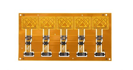
4 layer Flex Circuit with HDI


Challenges and Solutions

While HDI and via technologies bring numerous benefits, they also present challenges, such as:

  • Manufacturing Complexity: Precision is crucial when drilling and plating microvias, blind vias, and buried vias.
  • Cost Implications: HDI PCBs are costlier to manufacture due to their intricate processes and specialized materials.
  • Thermal Stress: Smaller vias can be more prone to stress under high temperatures.

To address these challenges, manufacturers adopt advanced techniques such as laser drilling for microvias, high-quality materials for improved durability, and stringent quality control processes to ensure reliability.


Conclusion

The integration of HDI technology with blind and buried vias has revolutionized complex PCB manufacturing. By enabling compact, high-performance designs, these technologies are driving innovation across industries, from consumer electronics to automotive and medical devices. As the demand for miniaturized, high-functionality products continues to grow, the role of HDI technology in PCB manufacturing will only become more significant. Manufacturers who invest in mastering these advanced techniques are poised to lead the way in next-generation electronic design and production.


HDI PCB manufacturer stackup


XPCB Limited: Advanced PCB Manufacturing to Simplify Your Journey


Navigating the complexities of PCB production has never been easier. XPCB Limited combines advanced PCB manufacturing technology with streamlined processes to offer solutions that meet your exact requirements. From prototypes to mass production, we are committed to quality, speed, and affordability. Trust XPCB Limited to make your PCB journey simple and successful.
Share

Related posts

dispensing in PCB
2025-02-07

Multilayer PCB Assembly and HDI PCB Manufacturing for High-Tech Solutions


Read more
smt product line
2025-02-06

Streamline Your PCB Production with XPCB’s Turnkey PCBA Services


Read more
2025-02-05

Comprehensive Turnkey PCBA Services: From BOM to SMT Assembly


Read more
amazon
amphenol-logo
halliburton
intel logo
samtec logo
sanmina logo

Company Info

XPCB Limited is a premium PCB & PCBA manufacturer based in China.

We specialize in multilayer flexible circuits, rigid-flex PCB, HDI PCB, and Rogers PCB.

Quick-turn PCB prototyping is our specialty.  Demanding project is our advantage.

Head Office

XPCB Limited
Address :
Building 3, JinFeng Industry Area,  Fuyong Town, Baoan District, Shenzhen, Guangdong, 518103, China.

Tel : +86-136-3163-3671
Fax : +86-755-2301 2705
Email : [email protected]

Quick Links

  • Flexible PCB
  • Rigid Flex PCB
  • ELIC HDI PCB
  • RF PCB
  • PCB Capability
  • PCBA Capabiility
  • About Us

PCB Blog

Multilayer PCB Assembly and HDI PCB Manufacturing for High-Tech Solutions

Read More »

Streamline Your PCB Production with XPCB’s Turnkey PCBA Services

Read More »

Comprehensive Turnkey PCBA Services: From BOM to SMT Assembly

Read More »

© 2024 - XPCB Limited All Right Reserve