• +86-755-23012705
  • Building 3, Jinfeng Industrial Park, Fuyong Street, Baoan District, Shenzhen ,China
  • [email protected]
logo
  • Home
  • About Us
    • Flexible PCB Fabrication
    • PCB Fab Capability
    • Our Certifications
    • Our Facility
    • Quality Assurance
  • PCB Fabrication
    • Flexible PCB
    • Rigid Flex PCB
    • Rigid PCB
    • ELIC HDI PCB
    • RF PCB
    • Medical PCB
    • Automotive PCB
    • IoT & IIoT PCB
    • Industrial Control PCB
    • Telecommunication PCB
    • Consumer Electronics PCB
  • PCB Assembly
    • Turn Key PCB Assembly
    • Consigned PCB Assembly
    • Components Sourcing
  • Resources
    • PCB Glossary
    • PCB Design Guide
    • PCB Blog
  • Contact
  • Home
  • About Us
    • Flexible PCB Fabrication
    • PCB Fab Capability
    • Our Certifications
    • Our Facility
    • Quality Assurance
  • PCB Fabrication
    • Flexible PCB
    • Rigid Flex PCB
    • Rigid PCB
    • ELIC HDI PCB
    • RF PCB
    • Medical PCB
    • Automotive PCB
    • IoT & IIoT PCB
    • Industrial Control PCB
    • Telecommunication PCB
    • Consumer Electronics PCB
  • PCB Assembly
    • Turn Key PCB Assembly
    • Consigned PCB Assembly
    • Components Sourcing
  • Resources
    • PCB Glossary
    • PCB Design Guide
    • PCB Blog
  • Contact
Get Instant Quote

Basic Knowledge Of Manufacturing Blind Via Circuit Boards.

15980684071 Basic Knowledge Of Manufacturing Blind Via Circuit Boards.


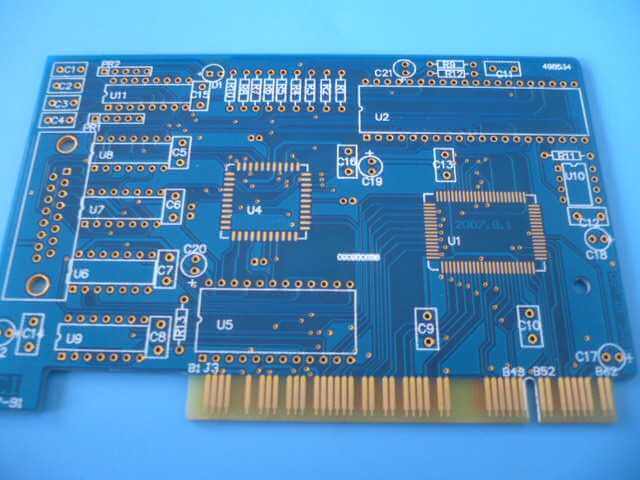
What is a blind via PCB circuit board? 


The so-called blind hole circuit board refers to the hole that is not drilled, the difference between a blind hole and a through hole is that the through hole is the hole that is drilled through all layers, and the blind hole is drilled before pressing, and the through hole is drilled after pressing.


What basic knowledge do you need to know to make blind-hole PCB circuit boards?

(1) Drill belt: Select through hole as the unit reference hole, each blind hole drill belt needs to select a hole, identify its corresponding unit reference hole coordinates, and note which drill belt corresponds to which layers, when the laser hole and the inner layer of the buried hole together, even if the hole of the two drill strips is in the same position, it is also necessary to confirm with the customer, move the position of the laser hole to ensure the electrical connection, can not be arbitrarily dealt with by experience.

(2) Tooling holes: The inner layer of the ordinary multi-layer board does not need to be drilled, only when making blind hole circuit boards, all tooling holes of blind hole boards are drilled, and the edge of the production panel needs to be drilled to distinguish each board.

(3) Film modification: Remark that the film produces a positive and negative film, the plate thickness is greater than 8mil (without copper) and the positive film process is taken, and the negative film process is less than 8mil (without copper), and the copper thickness at d/f should be considered when the line thickness/line gap valley is large, rather than the bottom copper thickness.

AOI machine


(4) Production process: The only difference between the blind hole plate and the buried through hole is that one side is in the outer layer, and it is necessary to do single-sided D/F and pay attention not to turn the wrong surface (when the double-sided bottom copper is inconsistent); When D/F is exposed, the bright copper surface is covered with black tape to prevent light transmission, because the blind hole plate is on the surface of the plate and the other is on the inner layer.


Your Trusted Partner for PCB Success: XPCB Limited
Let XPCB Limited be your guide to PCB success. Our comprehensive PCB manufacturing, rapid prototyping, and turnkey PCBA services are designed to meet your needs with ease. Count on us to deliver reliable solutions that exceed your expectations. With XPCB Limited, your journey to PCB excellence starts here.

Share

Related posts

Gold finger PCB
2024-04-13

What Is The Difference Between PCB Immersion Gold And Gold Plating


Read more
China quick-turn rigid flex PCB manufacturer
2024-04-12

Do You Know Rapid Flex PCB Have 5 Benefits?


Read more
PCB design guidelines
2024-04-11

About PCB Diagram Design To 5 Frequently Questions


Read more
amazon
amphenol-logo
halliburton
intel logo
samtec logo
sanmina logo

Company Info

XPCB Limited is a premium PCB & PCBA manufacturer based in China.

We specialize in multilayer flexible circuits, rigid-flex PCB, HDI PCB, and Rogers PCB.

Quick-turn PCB prototyping is our specialty.  Demanding project is our advantage.

Head Office

XPCB Limited
Address :
Building 3, JinFeng Industry Area,  Fuyong Town, Baoan District, Shenzhen, Guangdong, 518103, China.

Tel : +86-136-3163-3671
Fax : +86-755-2301 2705
Email : [email protected]

Quick Links

  • Flexible PCB
  • Rigid Flex PCB
  • ELIC HDI PCB
  • RF PCB
  • PCB Capability
  • PCBA Capabiility
  • About Us

PCB Blog

What Is The Difference Between PCB Immersion Gold And Gold Plating

Read More »

Do You Know Rapid Flex PCB Have 5 Benefits?

Read More »

About PCB Diagram Design To 5 Frequently Questions

Read More »

© 2023 - XPCB Limited All Right Reserve