• +86-755-23012705
  • Building 3, Jinfeng Industrial Park, Fuyong Street, Baoan District, Shenzhen ,China
  • [email protected]
logo
  • Home
  • About Us
    • Flexible PCB Expertise
    • Our Certifications
    • Our Facility
    • Quality Assurance
  • PCB Fabrication
    • Flexible PCB
    • Rigid Flex PCB
    • Rigid PCB
    • ELIC HDI PCB
    • RF PCB
    • Medical PCB
    • Automotive PCB
    • IoT & IIoT PCB
    • Industrial Control PCB
    • Telecommunication PCB
    • Consumer Electronics PCB
  • PCB Assembly
    • Turn Key PCB Assembly
    • Consigned PCB Assembly
    • Components Sourcing
  • Capabilities
    • PCB Fab Capability
    • ATE PCB Fabrication
    • PCB Technology Roadmap
    • PCB Assembly Services
    • PCB Design Support
  • Contact
  • Resources
    • PCB Blog
    • PCB Glossary
Get Quote

Blind Via and Buried Via: Essential Technologies for Achieving High-Density Interconnections in Complex PCB Manufacturing

HDI PCB manufacturer stackup

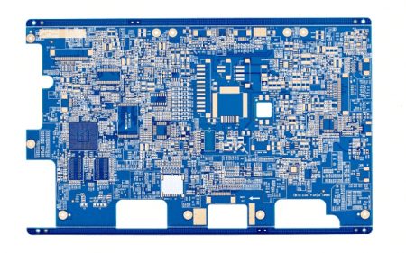
In the world of advanced electronics, the push for miniaturization and enhanced functionality has led to significant innovations in printed circuit board (PCB) design and manufacturing. Among these advancements, blind vias and buried vias stand out as essential technologies that enable the development of high-density interconnect (HDI) PCBs. These specialized via structures play a critical role in achieving compact, multi-layered designs with improved electrical performance. This blog delves into the importance of blind and buried vias in complex PCB manufacturing and how they contribute to high-density interconnections.


Understanding Blind and Buried Vias

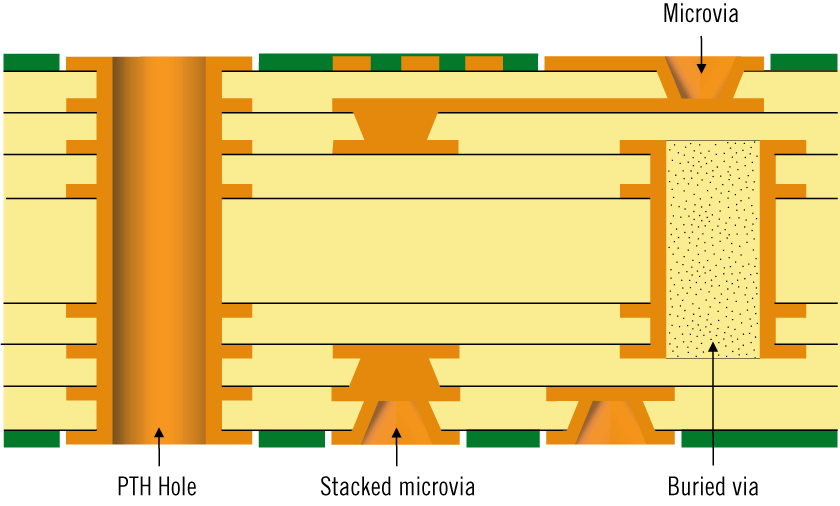
Vias are small holes drilled into a PCB to create electrical connections between layers. In traditional PCBs, through-hole vias pass entirely through the board. While effective, these vias occupy valuable space on all layers, limiting design flexibility and density. Blind and buried vias, however, offer advanced alternatives:

  • Blind Vias: Connect an outer layer of the PCB to one or more inner layers without passing through the entire board. These vias are “blind” because they are visible only on one side of the PCB.
  • Buried Vias: Connect two or more inner layers without reaching the outer layers. These vias are entirely “buried” within the board and invisible from the surface.

By minimizing surface disruption and optimizing layer interconnects, blind and buried vias enable designers to achieve more compact and efficient PCB layouts.


10L 1 Tier HDI Rigid PCB manufacturer


Advantages of Blind and Buried Vias

  1. Increased Design Flexibility:
    • Blind and buried vias free up surface space, allowing for the placement of more components and intricate routing paths.
    • This flexibility is particularly valuable in HDI PCBs, where dense component placement is crucial.
  2. Enhanced Signal Integrity:
    • Shorter signal paths reduce electrical interference and signal degradation, improving overall performance.
    • These vias support high-speed applications by minimizing parasitic inductance and capacitance.
  3. Compact PCB Designs:
    • By utilizing blind and buried vias, manufacturers can create multilayer boards with higher component densities and reduced size.
    • This is essential for modern devices like smartphones, wearables, and IoT gadgets.
  4. Improved Reliability:
    • Blind and buried vias reduce the risk of mechanical stress and warping, enhancing the durability of the PCB.


Manufacturing Challenges and Solutions

The fabrication of blind and buried vias requires advanced manufacturing techniques and precise control. Key challenges include:

  • Laser Drilling: Creating microvias with high accuracy demands sophisticated laser technology.
  • Layer Registration: Ensuring precise alignment of layers is critical to avoid connectivity issues.
  • Fill and Plating: Proper filling and plating of vias ensure electrical continuity and structural integrity.

To overcome these challenges, manufacturers employ state-of-the-art equipment and processes such as:

  • Laser drilling systems for precise microvia creation.
  • High-resolution imaging for accurate layer alignment.
  • Advanced electroplating techniques for reliable via filling and connectivity.


HDI rigid pcb suupplier


Applications of Blind and Buried Vias

Blind and buried vias are indispensable in a variety of industries and applications:

  1. Consumer Electronics:
    • Smartphones, tablets, and wearables benefit from the compactness and enhanced performance enabled by these vias.
  2. Automotive Electronics:
    • Advanced driver-assistance systems (ADAS), infotainment systems, and sensors rely on high-density PCBs for reliable operation.
  3. Medical Devices:
    • Miniaturized medical equipment, such as implantable devices and diagnostic tools, require the precision and density offered by blind and buried vias.
  4. Aerospace and Defense:
    • High-reliability applications, including avionics and communication systems, depend on the durability and performance of HDI PCBs.


Choosing the Right Manufacturing Partner

Implementing blind and buried vias requires expertise in HDI PCB manufacturing. When selecting a manufacturing partner, consider the following:

  • Technical Capabilities: Ensure the manufacturer has advanced equipment and proven experience in fabricating HDI PCBs with blind and buried vias.
  • Quality Standards: Look for certifications such as ISO 9001, IPC-6012, and RoHS compliance to guarantee high-quality production.
  • Comprehensive Services: A one-stop provider offering design support, fabrication, assembly, and testing can streamline the production process.


6 layer HDI rigid flex PCB


Final Thoughts

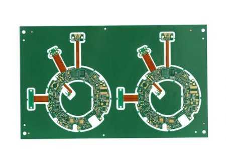
Blind and buried vias are essential technologies for achieving high-density interconnections in complex PCB manufacturing. By optimizing space utilization and enhancing electrical performance, these vias enable the creation of compact, high-performance electronic devices that meet the demands of today’s market.

Whether you are designing consumer electronics, automotive systems, or medical devices, leveraging blind and buried via technology can elevate your products to new heights. Partnering with a skilled and experienced PCB manufacturer ensures that your designs are brought to life with precision and reliability, paving the way for innovation and success.


XPCB Limited: Your Partner for Turnkey PCBA Services and Advanced PCB Solutions


Looking for a reliable partner to bring your PCB projects to life? XPCB Limited offers end-to-end turnkey PCBA services and advanced PCB manufacturing solutions. From prototype development to full-scale production, we ensure unparalleled quality and efficiency. Choose XPCB Limited to simplify your workflow and achieve outstanding results for every project.


Share

Related posts

dispensing in PCB
2025-02-07

Multilayer PCB Assembly and HDI PCB Manufacturing for High-Tech Solutions


Read more
smt product line
2025-02-06

Streamline Your PCB Production with XPCB’s Turnkey PCBA Services


Read more
2025-02-05

Comprehensive Turnkey PCBA Services: From BOM to SMT Assembly


Read more
amazon
amphenol-logo
halliburton
intel logo
samtec logo
sanmina logo

Company Info

XPCB Limited is a premium PCB & PCBA manufacturer based in China.

We specialize in multilayer flexible circuits, rigid-flex PCB, HDI PCB, and Rogers PCB.

Quick-turn PCB prototyping is our specialty.  Demanding project is our advantage.

Head Office

XPCB Limited
Address :
Building 3, JinFeng Industry Area,  Fuyong Town, Baoan District, Shenzhen, Guangdong, 518103, China.

Tel : +86-136-3163-3671
Fax : +86-755-2301 2705
Email : [email protected]

Quick Links

  • Flexible PCB
  • Rigid Flex PCB
  • ELIC HDI PCB
  • RF PCB
  • PCB Capability
  • PCBA Capabiility
  • About Us

PCB Blog

Multilayer PCB Assembly and HDI PCB Manufacturing for High-Tech Solutions

Read More »

Streamline Your PCB Production with XPCB’s Turnkey PCBA Services

Read More »

Comprehensive Turnkey PCBA Services: From BOM to SMT Assembly

Read More »

© 2024 - XPCB Limited All Right Reserve