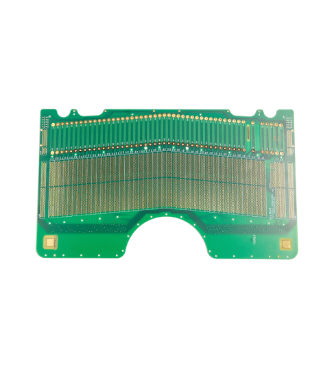


The continuous evolution of electronics has spurred demand for smaller, faster, and more efficient devices, driving innovation in printed circuit board (PCB) design and manufacturing. Among the key advancements enabling high-density interconnect (HDI) PCBs are blind via and buried via technologies. These techniques allow manufacturers to increase the number of connections within a PCB without increasing its size. However, implementing these technologies in high-end complex PCBs is not without its challenges. Below, we explore the key obstacles and potential solutions.
1. Manufacturing Complexity: Blind vias (vias that connect an outer layer to one or more inner layers) and buried vias (vias confined entirely within the inner layers) require precise manufacturing processes. These vias necessitate advanced drilling techniques, such as laser drilling, which can be costly and time-consuming. Misalignments during drilling can lead to defective connections and compromise the PCB’s performance.
2. Cost Implications: The integration of blind and buried vias significantly increases production costs. The need for additional processing steps, such as multiple lamination cycles and advanced drilling, adds to manufacturing expenses. This cost factor is a critical consideration for both designers and manufacturers, particularly when scaling production.
3. Thermal Management Issues: High-density PCBs with blind and buried vias often face challenges related to heat dissipation. Poor thermal management can lead to hotspots, reducing the reliability and lifespan of the PCB. Ensuring adequate heat dissipation becomes increasingly complex as the board’s density increases.
4. Signal Integrity Concerns: Signal integrity is a major concern in high-frequency applications. Improperly designed blind and buried vias can introduce impedance mismatches, signal losses, and crosstalk, negatively affecting the performance of high-speed circuits.
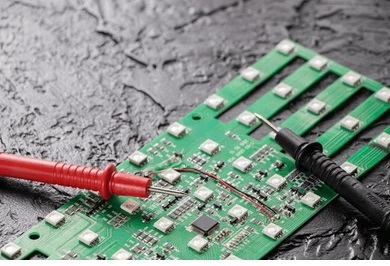
5. Inspection and Testing: Blind and buried vias are embedded within the PCB layers, making them difficult to inspect and test. Traditional inspection methods may not detect defects in these hidden structures, necessitating advanced inspection techniques, such as X-ray imaging, which add to production costs and complexity.
1. Advanced Drilling Techniques: Utilizing state-of-the-art drilling technologies, such as CO2 or UV laser drilling, can enhance the precision of via creation. These methods enable the formation of smaller vias with higher accuracy, reducing the risk of misalignment and defects.
2. Improved Lamination Processes: Multiple lamination cycles are often required to integrate blind and buried vias. Optimizing lamination parameters, such as pressure, temperature, and time, can improve layer bonding and via reliability. Investing in high-quality materials that can withstand these processes also helps ensure durability.
3. Enhanced Thermal Management Solutions: To address thermal challenges, designers can incorporate materials with higher thermal conductivity, such as metal core substrates or advanced thermal interface materials. Strategic placement of vias and the use of thermal vias can further aid in heat dissipation.
4. Signal Integrity Optimization: Advanced simulation tools can help predict and mitigate signal integrity issues during the design phase. Techniques such as controlled impedance routing, proper via stack-up design, and the use of back-drilling can minimize impedance mismatches and reduce signal losses.
5. Advanced Inspection and Testing Techniques: Investing in non-destructive testing methods, such as automated X-ray inspection (AXI) and 3D X-ray tomography, ensures thorough evaluation of blind and buried vias. These techniques enable manufacturers to identify and rectify defects before assembly, reducing the likelihood of field failures.
6. Collaboration and Training: Close collaboration between PCB designers and manufacturers is crucial for the successful implementation of blind and buried vias. Training production teams on the latest techniques and standards ensures that manufacturing processes are carried out effectively and efficiently.
As technology continues to evolve, several trends are shaping the future of blind and buried via technologies in high-end PCBs:
Blind via and buried via technologies are indispensable for manufacturing high-end complex PCBs, allowing for increased functionality and miniaturization. While these technologies present challenges, advancements in drilling techniques, material science, and inspection methods provide viable solutions. By addressing these challenges with innovative strategies, the industry can continue to meet the growing demands for compact, high-performance electronic devices.
XPCB Limited: Your One-Stop Solution for PCB Manufacturing and Assembly
XPCB Limited is your one-stop solution for all your PCB manufacturing and assembly needs. From design and prototyping to full-scale production, we offer comprehensive services under one roof. With a focus on quality, efficiency, and customer satisfaction, we make it easy for you to complete your projects with confidence. Simplify your PCB process today with XPCB Limited.
XPCB Limited is a premium PCB & PCBA manufacturer based in China.
We specialize in multilayer flexible circuits, rigid-flex PCB, HDI PCB, and Rogers PCB.
Quick-turn PCB prototyping is our specialty. Demanding project is our advantage.
Tel : +86-136-3163-3671
Fax : +86-755-2301 2705
Email : [email protected]
© 2024 - XPCB Limited All Right Reserve
