


Surface Mount Device (SMD) packaging has become the standard for modern electronic assembly due to its numerous advantages, including smaller size, high-density circuit designs, and cost-effectiveness. However, despite these benefits, SMD packaging comes with its own set of challenges. As electronics continue to evolve, understanding these challenges is crucial for engineers and designers to make informed decisions and ensure optimal product performance. In this blog, we will explore some of the common challenges faced in SMD packaging and how to overcome them.
One of the primary advantages of SMD technology is the ability to create compact and miniaturized electronic devices. However, this miniaturization also brings about several challenges. As components become smaller, it becomes increasingly difficult to handle and place them accurately on the PCB.
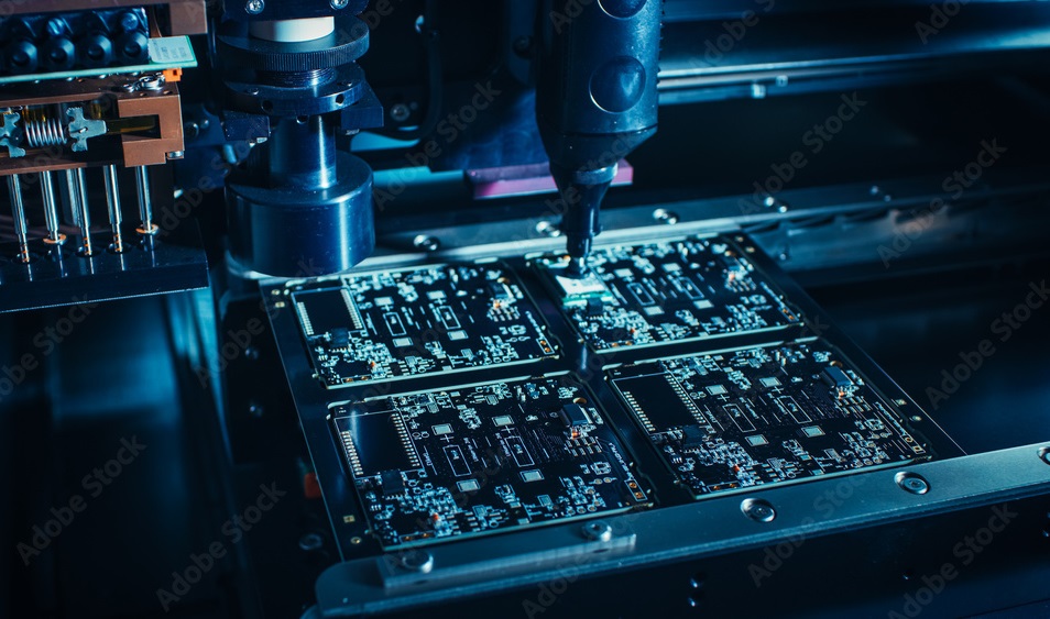
Challenge: With smaller components, there is a greater risk of misalignment or improper placement during assembly, especially when using automated pick-and-place machines. Additionally, handling and inspecting these tiny components manually can be challenging, increasing the potential for errors during the manufacturing process.
Solution: To address this challenge, automated assembly processes, such as advanced pick-and-place machines with precise vision systems, are essential. These machines can place components with high accuracy, reducing the risk of misalignment. Additionally, adopting higher-precision inspection techniques, such as automated optical inspection (AOI), can help detect placement issues before moving on to the soldering process.
Soldering is a critical step in the assembly of SMD components, as it ensures the electrical connections between the component leads and the PCB. However, SMD soldering presents its own set of challenges, particularly in the areas of solder joint quality and consistency.
Challenge: Soldering SMD components, especially small packages such as 0402 or 0201, can be difficult. These tiny components are highly sensitive to the soldering process, and improper temperature profiles or solder paste application can lead to issues like cold solder joints, bridging, or insufficient solder. Poor solder joints can result in unreliable electrical connections, which can cause circuit failure.
Solution: To overcome soldering challenges, manufacturers rely on precise reflow soldering techniques. Reflow soldering involves melting solder paste on the PCB to create secure connections between the component leads and the board. To ensure high-quality solder joints, it’s crucial to use the correct solder paste and to maintain an optimal temperature profile during the reflow process. Additionally, using advanced soldering technologies such as laser soldering or selective soldering can help mitigate some of the challenges associated with small or delicate components.

Effective thermal management is a significant concern in SMD packaging, especially as devices become more powerful and compact. As more components are packed onto smaller PCBs, the heat generated by these components can become a critical issue.
Challenge: The smaller size of SMD components means there is less surface area for heat dissipation. When components such as processors, power transistors, and high-power LEDs are mounted in close proximity, the heat generated by one component can affect the performance and longevity of others. This can lead to overheating, reduced efficiency, and even failure of the components.
Solution: To address thermal management challenges, engineers can use several strategies. One solution is to use SMD components with built-in thermal pads or heatsinks to help dissipate heat more effectively. Additionally, improving the layout of the PCB to allow better airflow and using materials with better thermal conductivity can also help. For high-power applications, more advanced solutions such as forced air cooling or liquid cooling may be necessary.
With the wide variety of SMD components available, ensuring that components are compatible with one another and with the overall design can be a challenge. Different components come in different package types, pin configurations, and sizes, which may make it difficult to integrate them into a single design.
Challenge: Incompatibility between component packages, especially with varying lead pitches or package heights, can cause difficulties during assembly and impact the overall performance of the circuit. Additionally, mismatches in electrical characteristics between components can lead to suboptimal performance or failure.
Solution: To ensure compatibility, designers should carefully select components that are specifically suited for the intended application and ensure they meet the required specifications. Using simulation tools during the design phase can also help identify potential compatibility issues before production begins. Furthermore, component standardization within a design can help reduce the chances of incompatibility.
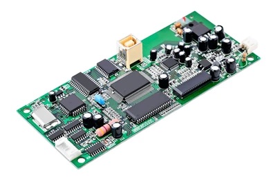
Designing a PCB for SMD components can be more complex than designing for through-hole components. The compact nature of SMDs and their specific mounting requirements place constraints on the layout of the PCB.
Challenge: As component density increases, the available space on the PCB decreases, making it more difficult to route traces without causing interference or signal degradation. Additionally, small packages often have tighter tolerances for pad sizes and spacing, which can increase the complexity of the PCB layout.
Solution: To overcome these challenges, careful planning and optimization during the PCB layout phase are critical. Engineers must ensure that the PCB design adheres to strict design rules regarding trace widths, pad sizes, and component placement. Utilizing advanced PCB design software that includes automatic design rule checks (DRC) can help identify potential issues early in the design process. Additionally, using multi-layer PCBs can help accommodate higher component densities by providing more space for routing traces.
SMD components are smaller and more densely packed than through-hole components, which can make them harder to inspect for defects. Manual inspection of SMD components can be difficult due to their size, and relying solely on human inspection can lead to missed defects.
Challenge: Detecting defects such as misalignment, soldering issues, or component damage can be more challenging in SMD packages. If undetected, these issues can lead to circuit failures or performance degradation.
Solution: To address inspection challenges, automated optical inspection (AOI) systems are often used. AOI systems use cameras and advanced software to inspect solder joints, component placement, and alignment, ensuring that the assembly process meets the required standards. X-ray inspection may also be used for more complex SMD packages, such as BGA (Ball Grid Array) components, where hidden solder joints are difficult to inspect visually.
While SMD packaging offers many advantages in terms of miniaturization, high-density designs, and manufacturing efficiency, it also comes with its share of challenges. From issues with soldering and thermal management to component compatibility and PCB design constraints, overcoming these challenges requires a combination of careful planning, advanced manufacturing technologies, and rigorous quality control processes. As the demand for smaller, more powerful electronic devices continues to grow, addressing these challenges will remain a key focus for engineers and manufacturers in the electronics industry. By leveraging innovative solutions and staying ahead of emerging technologies, it is possible to mitigate these challenges and continue pushing the boundaries of what SMD packaging can achieve.
Your Trusted Partner for PCB Success: XPCB Limited
Let XPCB Limited be your guide to PCB success. Our comprehensive PCB manufacturing, rapid prototyping, and turnkey PCBA services are designed to meet your needs with ease. Count on us to deliver reliable solutions that exceed your expectations. With XPCB Limited, your journey to PCB excellence starts here.
XPCB Limited is a premium PCB & PCBA manufacturer based in China.
We specialize in multilayer flexible circuits, rigid-flex PCB, HDI PCB, and Rogers PCB.
Quick-turn PCB prototyping is our specialty. Demanding project is our advantage.
Tel : +86-136-3163-3671
Fax : +86-755-2301 2705
Email : [email protected]
© 2024 - XPCB Limited All Right Reserve
