


How to identify the number of layers of a PCB multi-layer board? We XPCB Limited will explain to you the identification method of multi-layer boards!
The 4-layer PCB of the pcb is the first and fourth layers of wiring, and the other layers have other uses (ground wire and power supply).
6 and 8 layers addes auxiliary signal layer.
PCB board design issues. Each layer has its own role. There is power layer, main signal layer, auxiliary signal layer, and ground layer. The general design of the 6 and 8 layers is the same.
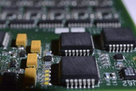
The substrate of the PCB board is made of insulating and heat-insulating materials that are not easy to bend. The small circuit material that can be seen on the surface is copper foil. The copper foil is originally covered on the entire PCB board, but part of it is etched away during the manufacturing process, and the remaining part becomes a net-like small circuit.
These lines are called wires or wiring, and are used to provide circuit connections for parts on the PCB. Usually the color of PCB board is green or brown, which is the color of solder mask. It is an insulating protective layer that can protect the copper wire and prevent parts from being welded to the wrong place.
Multilayer boards are now used on motherboards and graphics cards, greatly increasing the area that can be wired. Multilayer boards use more single or double-layer wiring boards, and put ainsulating layer between each layer of boards and press them together. The number of layers of the PCB board means that there are several independent wiring layers. Usually the number of layers is even and contains the two outermost layers. Common PCB boards generally have a structure of 4 to 8 layers. The number of layers of many PCB boards can be seen by looking at the cut surface of the PCB board. But in fact, no one can have such good eyesight. So, let me teach you one more method below.
The circuit connection of the multi-layer board is through buried via and blind via technology. Most motherboards and display cards use 4-layer PCB boards, and some use 6, 8-layer, or even 10-layer PCB boards. If you want to see how many layers the PCB has, you can identify it by observing the via holes, because the 4-layer boards used on the motherboard and display card are traces on the first and fourth layers, and the other layers have other uses (ground wires and power supply). Therefore, like the double-layer board, the via hole will penetrate the PCB board. If some vias appear on the front of the PCB but cannot be found on the reverse, then it must be a 6/8-layer board. If the same via holes can be found on both sides of the PCB, it will naturally be a 4-layer board.
Tips: Point the motherboard or display card to the light source. If the position of the guide hole can transmit light, it means that it is a 6/8-layer board. Otherwise, it is a 4-layer board.
PCB is short for Print Circuit Board. It is to attach a conductive copper sheet on a substrate of insulating material to be used as a circuit connection. These circuit connections can be on the front, back, or even in the middle of the substrate. Generally, PCBs with more than 2 layers (ie, front and back) circuit layers are called multilayer boards.
PCBs can be divided into single-layer boards (single-sided boards) with circuits printed on one side, double-sided boards with circuits printed on both sides, and multilayer boards with multilayer circuits in between.
XPCB Limited is a premium PCB & PCBA manufacturer based in China.
We specialize in multilayer flexible circuits, rigid-flex PCB, HDI PCB, and Rogers PCB.
Quick-turn PCB prototyping is our specialty. Demanding project is our advantage.
Tel : +86-136-3163-3671
Fax : +86-755-2301 2705
Email : [email protected]
© 2023 - XPCB Limited All Right Reserve
