- +86-755-23012705
- Building 3, Jinfeng Industrial Park, Fuyong Street, Baoan District, Shenzhen ,China
- [email protected]
Menu
Power PCB layout and wiring
In many cases, the current required by digital circuits is not continuous, so there will be a surge current for some high-speed devices. If the power supply circuitries are very long, the presence of an inrush current will lead to high-frequency noise, which will be introduced into other signals. And will inevitably exist in high-speed circuit parasitic inductance and parasitic resistance and parasitic capacitance, so the high-frequency noise will eventually be coupled to other circuits, and as a result of the existence of parasitic inductance can also lead to wiring can withstand the waves surge current ability to drop, leading to a portion of the pressure drop, disability is likely to make the circuit. So it is very important to add a bypass capacitor in front of the digital device. The larger the capacitance is, the more energy it can transmit is limited by the transmission rate, so a combination of a large capacitor and a small capacitor is generally used to satisfy the full frequency range.


Avoid hot spot generation: Signal through-holes can generate VOIDs in the power layer and the underlying layer. Therefore, improper placement of the hole is likely to increase the current density in some areas of the power supply or ground plane. And these places where the current density increases are called hot spots. Therefore, we should try our best to avoid this situation when setting through holes, so as not to cut the plane and eventually cause EMC problems. Often, the best way to avoid hot spots is to place through holes in a mesh pattern so that the current density is uniform and the plane is not isolated, so the backflow path is not too long and therefore does not cause EMC problems.
Bending mode of PCB routing
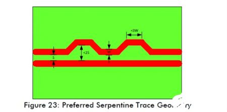
When laying the high-speed signal line, the signal line should avoid bending as far as possible. If you have to bend the line, do not use sharp or right angles. Instead, use obtuse angles. In the layout of high-speed signal lines, we often through the snake line to achieve the same length, the same snake line is actually a bending of the line. Line width, spacing, and bending mode should be made a reasonable choice, spacing should meet the 4W/1.5W rule.


The proximity of the signal
If the distance between high-speed signal lines is too close, it is easy to produce crosstalk. Sometimes, because of the layout, frame size and other reasons, the distance between the high-speed signal lines exceed our minimum requirements, so we have to increase the distance between the high-speed signal lines near the bottleneck. In fact, if space is enough to allow, try to increase the distance between the two high-speed signal lines.

PCB routing stubs
Long stub lines act as an antenna and can cause serious EMC problems if mishandled. At the same time, stub lines also cause reflection, reducing the integrity of the signal. Stub wires are most likely to be generated when pull-up or pull-down resistors are added to high-speed signal lines, and stub wires can be used to process stub wires. As a rule of thumb, this becomes a problem if the stub line is longer than 1/10 of a wavelength and can be used as an antenna.

Impedance discontinuity
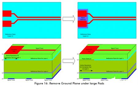
The impedance value of a trace generally depends on its line width and the distance between the trace and the reference plane. The wider the wire, the smaller the impedance. In some interface terminals or device pads, the same principle applies. When the pad of an interface terminal is connected to a high-speed signal line, if the pad is very large and the high-speed signal line is very narrow, the large pad will have a small impedance, while the narrow wiring will necessarily have a large impedance. In this case, there will be impedance discontinuity, and the impedance discontinuity will produce a signal reflection. Therefore, in order to solve this problem, a copper sheet is placed under the large pad of the interface terminal or device, and the reference plane of the pad is placed in another layer, so as to increase the impedance and make the impedance continuous.
Perforations are another source of impedance discontinuity. To minimize this effect, unwanted copper sheeting for inner and through connection should be removed. In fact, such an operation can be eliminated at the time of design through CAD tools or contact PCB manufacturers to eliminate the unnecessary copper skin, to ensure the continuity of impedance.

Differential signal
For high-speed differential signal lines, we must ensure equal width and equal spacing to achieve specific differential impedance values. Therefore, the distribution of differential signal lines as far as possible ensures symmetry.
Do not place holes or components in differential lines. Places of holes or components in differential lines will cause EMC problems and impedance discontinuity.

Sometimes, some high-speed differential signal lines require serial coupling capacitors. The coupling capacitor also needs to be arranged symmetrically, and the package of the coupling capacitor should not be too large. It is recommended to use 0402 and 0603, and it is also acceptable. It is best not to use capacitors above 0805 or side-by-side capacitors.
In general, through-holes cause a large impedance discontinuity, so for high-speed differential signal pairs, through-holes should be minimized, and if through-holes are to be used, they should be arranged symmetrically.


Isometric problem
In some high-speed signal interfaces, such as buses, the arrival time and delay error between signal lines should be considered. For example, in a set of high-speed parallel buses, the arrival time of all data signal lines must be guaranteed within a certain time delay error to ensure its establishment time and maintain time consistency. In order to satisfy this requirement, we have to consider equivalence. However, the high-speed differential signal line must guarantee strict time delay for the two signal lines, otherwise, communication failure is likely. Therefore, in order to meet this requirement, the serpentine line can be used to achieve equal length, and then the time delay requirements can be satisfied.
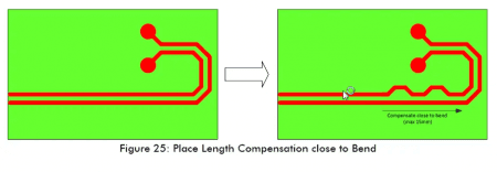
Serpentine lines should generally be placed at the source of the loss rather than at the distal end. It is at the source that the signals from the positive and negative ends of the different line are transmitted synchronously most of the time.

Wiring bending is one of the sources of the loss of length. For the wiring bend, its realization equal length should be close to the bend (<=15mm);
If two wires are bent and the distance between them is <=15mm, then the loss of length between them will compensate each other, so there is no need to do equal length processing.

For different parts of high-speed differential signal lines, they should be independent and equal in length. The through-hole, series-coupling capacitance, and interface terminal are two parts of the high-speed differential signal line, so special attention should be paid to this. Make sure they are equally long. Because a lot of EDA software in DRC is only concerned about whether the whole line is lost.
For interfaces such as LVDS display devices, there will be a number of pair difference pairs at the same time, and the timing sequence requirements between the different pairs are usually very strict, and the time delay requirements are very small. Therefore, for such differential signals, we generally require compensation in the same plane. Because the signal speeds are different at different layers.


Some EDA software will also calculate the wiring inside the pad within the length when calculating the wiring length. If the length compensation is carried out at this time, the actual result will be lost. So pay special attention at this time, when using some EDA software.
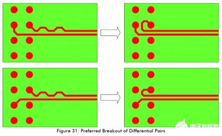
Always choose symmetrical outings if you can to avoid the need to end up with serpentine routing for equal length.

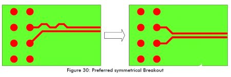
If space permits, try to add a small loop at the source of the short difference line to realize compensation, rather than through the serpentine line to compensate.


XPCB Limited is a premium PCB & PCBA manufacturer based in China.
We specialize in multilayer flexible circuits, rigid-flex PCB, HDI PCB, and Rogers PCB.
Quick-turn PCB prototyping is our specialty. Demanding project is our advantage.
Tel : +86-136-3163-3671
Fax : +86-755-2301 2705
Email : [email protected]
© 2023 - XPCB Limited All Right Reserve
