

In the world of modern electronics, the demand for smaller, faster, and more powerful devices is ever-increasing. As consumers and industries demand high-performance gadgets with more functionality in smaller packages, manufacturers must find innovative ways to meet these expectations. One of the key technologies that has facilitated this trend in Printed Circuit Board Assembly (PCBA) is High-Density Interconnect (HDI). HDI technology is a significant enabler of miniaturization and functional integration in PCBA, allowing for more complex and efficient designs. In this blog, we’ll explore how HDI technology is revolutionizing PCBA manufacturing and driving the next wave of electronic innovation.
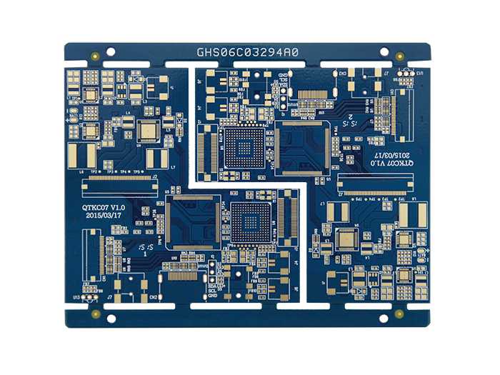
High-Density Interconnect (HDI) refers to a type of PCB that uses advanced techniques to create a higher component density on a smaller board. HDI PCBs utilize microvias (small holes), finer trace widths, and tighter spacing to accommodate more components within the same physical area, compared to traditional PCBs. This makes HDI ideal for applications requiring compact, high-performance electronic circuits, such as smartphones, tablets, wearables, and medical devices.
HDI technology typically includes features such as:
Microvias: Very small drilled holes used to connect different layers of the PCB.
High-density traces: Ultra-fine traces that allow for more efficient use of the available space.
Multiple layers: HDI boards often incorporate multiple layers to fit complex circuits in a small footprint.
Now, let’s explore how HDI technology supports miniaturization and functionality integration.
One of the primary advantages of HDI technology is its ability to enable miniaturization without sacrificing performance. As consumer devices become smaller, the components within them must also shrink. HDI allows for highly compact designs, reducing the overall size of the PCB and, consequently, the entire electronic device.
In traditional PCBs, larger components and wider traces require more space. With HDI, the use of microvias and fine traces allows for more components to be packed into a smaller area, facilitating smaller board sizes. This is especially important in industries like consumer electronics, where the trend is toward more compact, portable devices. For example, in smartphones, tablets, and wearable technology, HDI technology enables the reduction of board sizes while maintaining or improving performance.
Additionally, miniaturization with HDI helps reduce the weight of devices, making them more comfortable to carry and handle. Whether it’s a small medical device or a portable gaming console, the ability to make electronic components smaller, lighter, and more efficient is crucial to meeting modern consumer expectations.
As technology advances, the need for more functions in smaller devices grows. HDI technology helps meet this demand by supporting functional integration—the ability to combine multiple electronic functions into a single, compact unit. By using multiple layers and microvias to connect different sections of a PCB, HDI enables the integration of complex circuits and systems on a smaller footprint.
This functional integration allows manufacturers to consolidate components that might traditionally be found on separate boards into a single HDI PCB. For example, a single HDI PCB can integrate the microprocessor, memory, power management circuits, wireless communication modules, and other essential components. This reduces the number of individual parts needed and simplifies the overall design process.
In addition, HDI boards allow for the integration of advanced features such as sensors, Bluetooth modules, GPS, and other wireless capabilities without significantly increasing the size of the PCB. As the trend toward multifunctional devices grows, HDI technology becomes increasingly important in providing the necessary density and complexity for these integrated systems.
HDI technology also plays a critical role in improving the performance and reliability of PCBs. By using finer traces and smaller vias, HDI reduces the electrical resistance and improves signal integrity. This is especially important for high-speed circuits, which are common in modern electronics, as smaller traces and optimized vias help prevent signal loss, reduce interference, and enhance overall performance.
Moreover, HDI PCBs are typically made with higher-quality materials that ensure better durability and heat dissipation. This leads to improved reliability, making HDI technology ideal for applications that require long-lasting and high-performance circuits, such as medical devices, automotive electronics, and aerospace components.
The ability to reduce signal loss and interference in smaller devices is crucial in ensuring that advanced features, like wireless communication and high-speed data transfer, function properly. HDI technology allows manufacturers to create more reliable, high-performance devices while still adhering to size limitations.
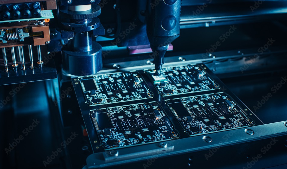
One of the challenges in developing small, complex devices is creating prototypes that can test multiple features and functions before full-scale production. HDI technology allows for more complex designs and flexible prototyping due to its ability to accommodate multiple layers and dense component placement. Designers can incorporate more functionality into a smaller prototype, reducing the need for multiple prototypes or design iterations.
The ability to test complex designs early in the development process can also reduce time-to-market, helping manufacturers stay competitive in fast-moving industries.
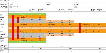
While HDI technology offers many benefits in terms of miniaturization and functional integration, it’s important to consider the associated costs. The complexity of HDI boards—due to fine-pitch components, microvias, and multi-layer designs—can increase production costs. HDI PCBs often require more sophisticated manufacturing processes and materials, which can be more expensive than traditional PCBs.
However, as demand for smaller, multifunctional devices grows, the cost of HDI manufacturing is expected to decrease over time, making it more accessible for a wider range of applications. The long-term benefits in terms of device size, performance, and functionality often outweigh these initial cost challenges, particularly for high-end consumer electronics and critical applications.
HDI technology is a powerful enabler of miniaturization and functional integration in PCBA, allowing manufacturers to pack more components and capabilities into smaller, more efficient designs. From smartphones to wearables, medical devices to automotive electronics, HDI is driving the development of next-generation products that are smaller, faster, and more feature-rich than ever before. By enhancing performance, improving reliability, and enabling complex multi-functional designs, HDI technology is at the heart of modern electronics manufacturing, supporting the miniaturization trend while meeting the growing demand for high-performance, multi-functional devices. As the technology continues to evolve, it will undoubtedly remain a critical enabler in the race toward ever-smaller and more powerful electronic devices.
Discover a World of Possibilities with XPCB Limited
At XPCB Limited, we’re here to help you explore new horizons. Our advanced PCB manufacturing, rapid prototyping, and turnkey PCBA solutions make it easy for you to turn your ideas into reality. Trust us to deliver excellence and reliability every step of the way. Join us and experience the power of innovation with XPCB Limited by your side.
XPCB Limited is a premium PCB & PCBA manufacturer based in China.
We specialize in multilayer flexible circuits, rigid-flex PCB, HDI PCB, and Rogers PCB.
Quick-turn PCB prototyping is our specialty. Demanding project is our advantage.
Tel : +86-136-3163-3671
Fax : +86-755-2301 2705
Email : [email protected]
© 2024 - XPCB Limited All Right Reserve
