


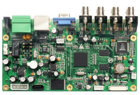
PCB copy board is usually called PCB imitation or PCB cloning. Simply put, it is to copy and clone the same or similar pcb board through electronic products. The whole process of copying pcb board requires certain technology and process operation method. Let me introduce you in detail.
PCB copy board is a reverse engineering of PCB design. First removes the components on the Printed circuit board to make a BOM list, scans the empty board into a picture and restores it to a pcb board drawing file through the copying software. Send the pcb board drawing file to the PCB factory to produce the board (PCBA), and then add the components (purchase the corresponding components according to the BOM list), which is exactly the same printed circuit board as the original printed circuit board.
Copy board is also called board modification, which is to conduct reverse technology research on the designed PCB board. After referring to a lot of information, the process of copying the board is summarized as follows:
The first step is to get a piece of PCB. Record the model, parameters, and positions of all vital parts on the paper, especially the direction of the diode, the tertiary tube, and the direction of the IC gap. It is best to use a digital camera to take two photos of the location of the vital parts. The current printed circuit boards are getting more and more advanced. Some of the diode transistors above can not be noticed at all.
The second step is to remove all the components and remove the tin in the PAD hole. Clean the PCB with alcohol and put it into the scanner. When the scanner scans, you need to inscrease the scanned pixels slightly to get a clearer image. Then lightly polish the top and bottom layers with water gauze paper until the copper film is shiny, put them in the scanner, start PHOTOSHOP, and scan the two layers separately in color. Note that the PCB must be placed horizontally and vertically in the scanner, otherwise the scanned image cannot be used.
The third step is to adjust the contrast and brightness of the canvas to make the part with copper film and the part without copper film have a strong contrast, then turn the second image into black and white, and check whether the lines are clear. If not, repeat this step. If it is clear, save the picture as black and white BMP format files TOP.BMP and BOT.BMP. If you find any problems with the graphics, you can also use PHOTOSHOP to repair and correct them.
The fourth step is to convert the two BMP format files into PROTEL format files, and transfer two layers in PROTEL. For example, the positions of PAD and VIA that have passed through the two layers basically coincide, indicating that the previous steps are well done. If If there is a deviation, repeat the third step. Therefore, PCB copying is a work that requires patience, because a small problem will affect the quality and the degree of matching after copying.
The fifth step is to convert the BMP of the TOP layer to TOP.PCB. Pay attention to the conversion to the SILK layer, which is the yellow layer. Then you can trace the line on the TOP layer and place the device according to the drawing in the second step. Delete the SILK layer after drawing. Keep repeating until all the layers are drawn.
The sixth step is to import TOP.PCB and BOT.PCB in PROTEL, and combine them into one picture.
The seventh step is to use a laser printer to print the TOP LAYER and BOTTOM LAYER on the transparent film (1:1 ratio), and put the film on the PCB. In the last step, check it thoroughly for errors. If there are no problems, then it’s done.
Note: If it is a multilayer board, you need to carefully polish to the inner layer, and repeat the copying steps from the third to the fifth step. Of course, the naming of the graphics is also different. It depends on the number of layers. Generally, double-sided copying requires much simpler than multi-sided boards. Multi-sided copy boards are prone to misalignment. Therefore, multi-sided board copy boards must be especially careful (wherein the internal vias and non-vias are prone to problems).
XPCB Limited is a premium PCB & PCBA manufacturer based in China.
We specialize in multilayer flexible circuits, rigid-flex PCB, HDI PCB, and Rogers PCB.
Quick-turn PCB prototyping is our specialty. Demanding project is our advantage.
Tel : +86-136-3163-3671
Fax : +86-755-2301 2705
Email : [email protected]
© 2023 - XPCB Limited All Right Reserve
