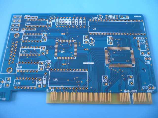
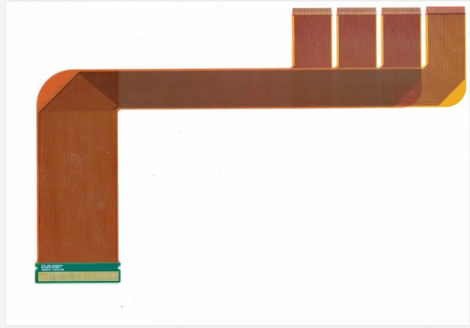
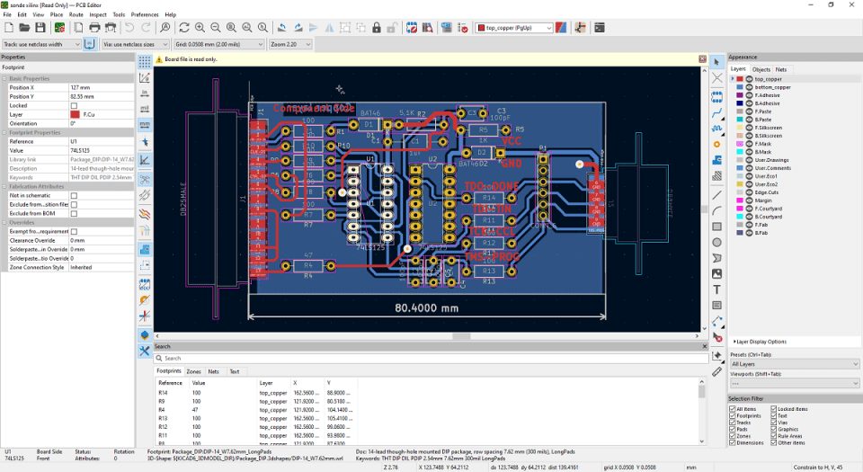
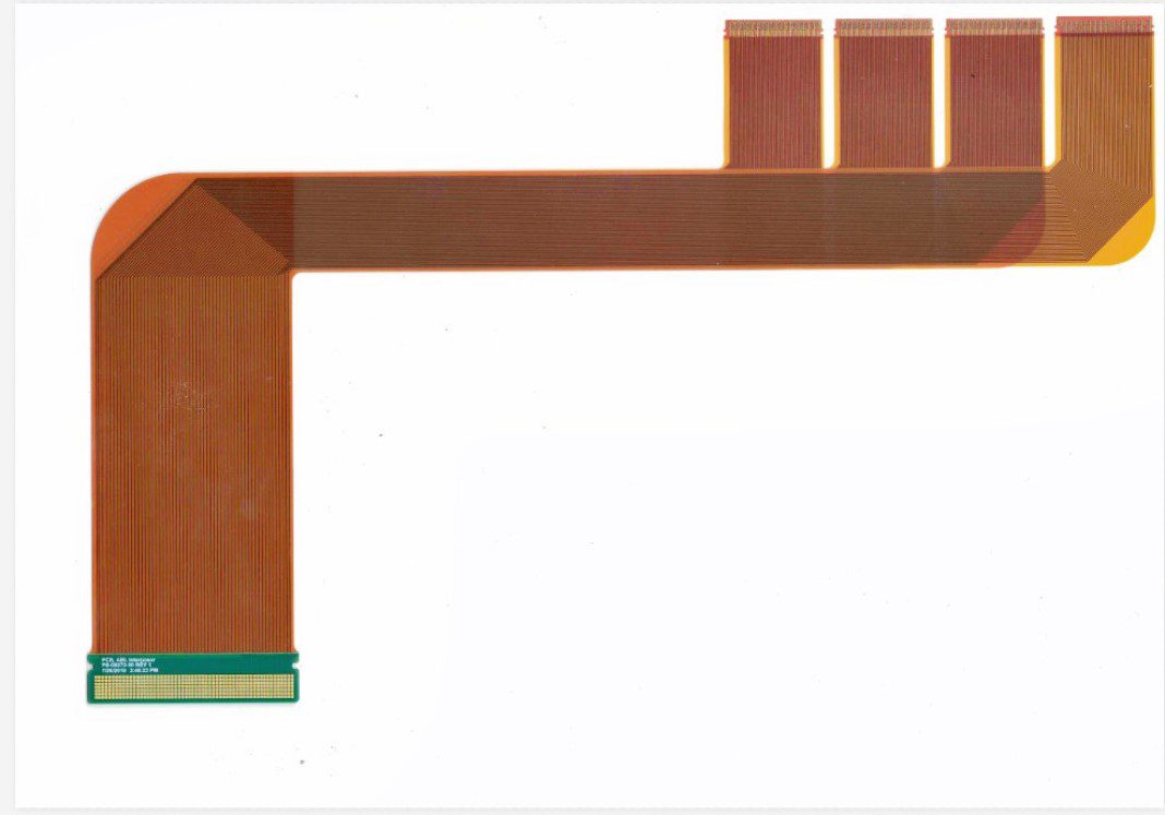
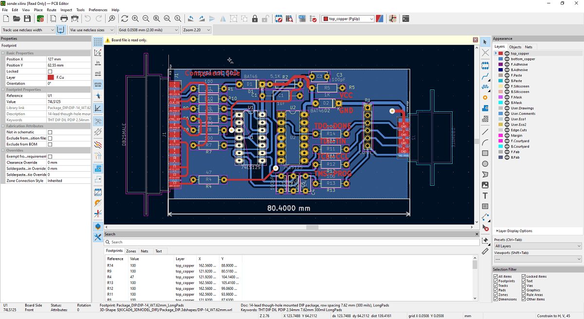
In an application, the cost of a printed circuit board has a huge impact on the overall price of the product. It is therefore important to include all steps that will help reduce this expenditure. Below are some steps you can take to reduce your overall application cost by making simple changes during the PCB design phase. Not only that, these steps will improve the efficiency of the PCB.
How to reduce PCB assembly cost?
The following steps can help you reduce PCB costs:
- It helps to use good drawing packaging at the assembly stage because it places the components on the PCB.
- You must use separate viewers for the Gerber and Excel files. Avoid using tools provided by design packages.
- When choosing a surface finish for your PCB, consult your PCB assembly service provider to avoid any conflicts.
- When placing a component on a board, you first need to place it in a specific position.
- The ideal space between PCB edge and component should be 100 mils.
- Similar components should be in the same direction on the board.
- Keep an even space between all components. Always consider horizontal and vertical Spaces.
- As far as possible, make sure the components are positioned at a 0 or 90 degree Angle.
- If double-sided PCB is used, the primary side should be used for intrinsically/functionally sensitive, heavy, or critical components. This rule also applies to through-hole components.
- Minimize the length of wiring as possible.