- +86-755-23012705
- Building 3, Jinfeng Industrial Park, Fuyong Street, Baoan District, Shenzhen ,China
- [email protected]
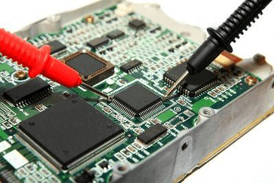
PCB in the process of production, hard to avoid the short circuit, open circuit and leakage caused by external factors, such as electrical flaws, coupled with the continuous toward high density PCB, fine spacing and the evolution of multi-level, and failure to timely to bad plate screening out, and let it go on the production process, is bound to cause waste more cost, so in addition to the improvement of the process control, improve test technology is also can offer the PCB maker to reduce scrap rate and improve product yield solutions.
In the production of electronic products, the cost loss caused by defects varies from stage to stage, and the earlier detection, the lower the cost of repair. The Rule of 10 “” is often used to estimate the cost of remedy-fixing a PCB when a defect is found in a different manufacturing process. For example, if the circuit breaks in the PCB Bare Board can be detected in real time after the production of the Board is completed, usually the defects can be improved by filling the lines, or at most one bare PCB board can be lost.
However, if the circuit fails to be detected, the downstream assembler will ask for compensation for the cost of spare parts, heavy industry fee and inspection fee from the hollow plate manufacturer after the plate is shipped to the downstream assembler to complete the parts installation and also through tin furnace and IR remelting. However, the circuit is found to be broken by the test at this time.
If more unfortunate, defective board in the assembler’s test is still not found, but into the overall system of finished products, such as computers, mobile phones, auto parts, etc., then do the test only to find the loss, will be light timely detected a hundred times, a thousand times, or even higher.
Therefore, electrical testing for PCB manufacturers is about early detection of functional defects in the circuit.
The downstream industry usually requires PCB manufacturer to do 100% electrical testing. Therefore, the PCB manufacturer and the PCB manufacturer will agree on the test conditions and test methods. Therefore, the following items will be clearly defined:

In each stage, there will usually be 2 to 3 times of 100% test to screen out the defective boards for heavy processing.
Therefore, the test station is also the best data collection source to analyze the problem points in the PCB manufacturing process. Through the statistical results, the percentage of circuit break, short circuit and other insulation problems can be obtained. After the heavy work, the test will be carried out again.

Electrical test is mainly to test the continuity and isolation of substrate lines. Conductivity test means to judge whether the circuit is disconnected by measuring whether the resistance value of the node in the same network is less than the threshold value of conduction, which is commonly called open circuit.
Insulation testing refers to the measurement of whether the resistance value between different network nodes is greater than the insulation threshold to determine whether the insulation network short circuit phenomenon.
With the increase of line density, the difficulty of electrical testing also increases, and new testing techniques are developed to cope with the development of PCB industry.
The main factors leading to the increased difficulty of the test include:
1) The size of PAD on the substrate surface
2) PAD span (Pitch)
3) Reduce wire spacing to reduce the conduction aperture
4) Surface indentation limit of PAD
5) The measurement stopping accuracy is required to be improved
6) Test speed requirement improvement and other factors
The methods of electrical testing are Dedicated, Universal Grid, Flying Probe, E-Beam, adhesive, Capacity and ATG-Scan MAN. The three most commonly used devices are Dedicated, general and ATG-scan machines.
To better understand the functions of each device, the features of the three major devices are compared below.
Specialized tests are specialized because the fixtures they use (such as circuit boards for electrical testing) only apply to one material number, so boards with different material Numbers can’t be tested and can’t be recycled. In terms of test points, the single panel can be tested within 10,240 points and 8,192 points on both sides. In terms of test density, it is more suitable for the board above pitch due to the thickness of the probe head.

Universal test is the basic principle of the layout of PCB circuitry is based on Grid (Grid) to design, generally the so-called line density is refers to the distance of the Grid, which is with spacing (Pitch) to represent (part time also can be said with hole density), and universal test is based on the principle of hole position based on the base of the G10 Mask, can only through the Mask in the position of the hole probe electric logging, so the fixture production simple and fast, and the probe can be reused.
General use test Standard Grid fixed large needle plates with many measuring points can produce active probe plates according to different material Numbers respectively. During mass production, as long as the active needle plates are changed, the mass production test can be carried out for different material Numbers.
In addition, in order to ensure the patency of PCB board line system, it is necessary to use the needle disk of specific contact to perform Open/Short electrical test on the board on the general electric measuring machine that USES high voltage (such as 250V) with multiple measuring points. Such general Testing machine is called “ATE” (Automatic Testing Equipment).
General test points are usually more than 10,000 points, test density in or test is called on-Grid test, if applied to high-density board, because the spacing is too close, has been out of on-Grid design, so belongs to off-Grid test, its fixture must be specially designed, usually general test density can reach QFP.
The principle of flying needle test is very simple, only two probes are needed to move X, Y and Z to test the two endpoints of each line one by one, so there is no need to make another expensive fixture.
However, due to the endpoint test, the measuring speed is very slow, about 10~40 points/ SEC, so it is more suitable for sample and small volume production.
In terms of test density, the flying needle test can be applied to extremely high-density PCB board, such as MCM.
A typical flying probe test yields between 1 and 20. If the hole density is known and can be converted to the total area tested per hour, the test area ranges from 15 (probe 20 and 32) to 0.04 (probe 1 and 600), with a difference of 375 times due to the density and spacing of the plates.
The average performance of the flying needle test equipment is maintained in the range of 10 to 15, suitable for commercial boards with density of 30 to 600 high density boards. For multi-layer PCB, in optimal condition each flying needle test machine tests a total area of approximately 3,000 to 5,000 square meter per year.
The bed-of-nails test equipment, such as special type and general type, is not as good as the flying needle test for high-density board, so it is less used for high-density board test. In theory, however, the needle disc production area of up to 200 ~ 400, but in terms of the present production situation, special on the actual production line is 30 ~ 100, and the universal is 15 ~ 50 (both comparison basis is special is usually applied to a large number of production, and universal used in small production), the theory and the actual difference except for the device itself factors, may also contain the problem on the production management, in this not to detail them.
Under general optimum conditions, the average number of specialized test equipment is about 300,000 per year and 150,000 for general use. However, the amount of output per unit may vary significantly depending on the PCB manufacturer’s production plan. For example, if the most advanced ATE testing cell phone board is used, each test equipment can produce about 600,000 per year, but if it is used for CSP of 0.5~0.8mm-pitch, the test rate is only about 1/4, and each test equipment can produce 150,000 per year.
It can be concluded from the above introduction. First of all, in terms of testing technology for purpose, flying probe test is the most suitable for use in small electrical test equipment of the production and samples, but if you want to use in a large number of production, is due to the slow speed as well as the equipment is expensive, will make the test cost is greatly increased, and the universal and special for what level of the board, as long as the output reaches a certain number of test cost all can achieve economies of scale standard, and accounts for only about 2-4% of the price, which is why universal and special for the current PCB test model of the main causes of the mass production.
But as the change of electronic products faster, makes the single circuit design version of the shorter product life cycle (e.g., the life cycle of the mobile plate is about 6 months), the phenomenon for PCB manufacturers in update the universal test fixture or dedicated testing equipment, all can bring high costs on threats, according to the data shows, if used in high density board, when average yields less than 150 square meters, the test cost will be higher than 18%, this is not the general can bear the cost of production, so the development trend of electronic products will be the PCB manufacturer when the choose and buy test equipment, a task that nots allow to ignore.
At present, e-Beam, CEM or Plasma Discharge technologies, which are still being actively improved, will be a good and feasible solution for electrical testing if the test efficiency can be improved.
Open circuit: A condition in which any two points in the same circuit should be energized, but the power is cut off.
Short circuit: A condition in which two conductors are not connected and should not be energized.
There are many reasons for an open short circuit. Different reasons show different characteristics, but one thing is common: there is no metal covering or no conduction in the conductive area, or there is metal covering or conduction in the non-conductive area. Theoretically, the above problems are generally caused by the following reasons.
With the rapid development of PCB industry, customers have increasingly strict requirements on enterprise delivery time. How to improve the test efficiency under the premise of ensuring product quality has become an important issue in the test process.
False open circuit and false short circuit are the most common interference phenomena in testing. How to eliminate false open circuit and false short circuit quickly is what every tester needs to master.

Through these years the development of the state as you can see, in order to satisfy the high density of electronic product development of PCB, the existing China PCB manufacturer’s test technology has been in a relatively backward status, to solve the existing problems of various test methods together at the same time, complement each other shortcomings, development of different types of PCB test equipment, can be a breakthrough in testing technology, meet the requirements of customers and PCB manufacturers. XPCB is an enterprise worthy of recommendation.


XPCB Limited is a premium PCB & PCBA manufacturer based in China.
We specialize in multilayer flexible circuits, rigid-flex PCB, HDI PCB, and Rogers PCB.
Quick-turn PCB prototyping is our specialty. Demanding project is our advantage.
Tel : +86-136-3163-3671
Fax : +86-755-2301 2705
Email : [email protected]
© 2024 - XPCB Limited All Right Reserve
