- +86-755-23012705
- Building 3, Jinfeng Industrial Park, Fuyong Street, Baoan District, Shenzhen ,China
- [email protected]
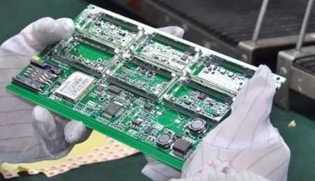
PCB layout is not a random thing, it has certain rules to follow. In addition to general requirements, some special devices may have different layout requirements.

1) There shall be no components higher than 3mm around the surface of bend/male and bend/mother compression devices, and there shall be no welding devices around 1.5mm;
The reverse side of the crimping device shall not have any components within 2.5mm of the pinhole center of the crimping device.
2) There shall be no components within 1mm around the straight/male, straight/mother compression device;
When the back of the straight/male, straight/mother compression device needs to be installed with jacket, no components shall be arranged within 1mm from the edge of jacket, and no components shall be arranged within 2.5mm from the compression hole without jacket.
3) The live plug and draw seat of the grounding connector with European connector. The cloth at the front end of the long needle is 6.5mm and the cloth at the short needle is 2.0mm.
4) The long PIN of the 2mmFB power supply with single PIN insertion corresponds to the 8mm forbidden cloth at the front end of the veneer socket.
1) In the layout of devices, thermosensitive devices (such as electrolytic capacitors, crystal oscillations, etc.) should be kept as far away from high-heat devices as possible.
2) The thermal sensitive device should be close to the element under test and far away from the high-temperature area, so as not to be affected by other equivalent components of thermal energy and cause wrong actions.
3) Place the hot and heat-resistant devices near the air outlet or on the top, but also near the air inlet if they cannot withstand high temperature, and pay attention to stagger the position with other heating devices and heat-sensitive devices in the direction of air rise as far as possible.
1) THD devices with polarity or directionality are in the same direction and arranged neatly in the layout.
2) The polar SMC should be in the same direction on the board as far as possible;
The same type of devices are arranged neatly and beautifully. (Polar devices include electrolytic capacitors, tantalum capacitors, diodes, etc.)
1) For PCB with non-transmitting edge size greater than 300mm, heavier components should not be placed in the middle of the PCB as far as possible, so as to reduce the influence of the weight of plug-in components on the DEFORMATION of PCB during the welding process and the influence of the plug-in process on the components already attached on the board.
2) For the convenience of insertion, the device is recommended to be placed near the operating side of insertion.
3) The length direction of devices with longer dimensions (such as memory strip sockets, etc.) is recommended to be consistent with the transmission direction.
4) The distance between the edge of the welding plate and QFP, SOP, connector and all BGA of pitch≤0.65mm is greater than 20mm.
The distance between SMT and other SMT devices is > 2mm.
5) the distance between the body of through-hole reflow welding device is > 10mm.
6) The distance between the edge of the welding plate and the transmitting edge of the through-hole reflow welding device is ≥10mm;
Distance ≥5mm from the non-transmitting edge.


XPCB Limited is a premium PCB & PCBA manufacturer based in China.
We specialize in multilayer flexible circuits, rigid-flex PCB, HDI PCB, and Rogers PCB.
Quick-turn PCB prototyping is our specialty. Demanding project is our advantage.
Tel : +86-136-3163-3671
Fax : +86-755-2301 2705
Email : [email protected]
© 2024 - XPCB Limited All Right Reserve
