


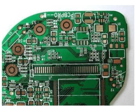
Many Different Process Flows of PCB Boards:
This article mainly introduces Double-sided tin-sprayed board, double-sided nickel-plated gold, multi-layer tin-sprayed board, multilayer nickel-plated gold, multilayer nickel-immersed gold board. The different process flow of these types of circuit boards are detailed Introduction.
1. Single Panel Process Flow
Cutting edge grinding → drilling → outer layer graphics → (full board gold plating) → etching → inspection → silk screen solder mask → (hot air leveling) → silk screen characters → shape processing → testing → inspection
2. Process Flow of Double-Sided Tin Spraying Board
Cutting edge grinding → drilling → heavy copper thickening → outer layer graphics → tin plating, etching tin removal → secondary drilling → inspection → screen printing solder mask → gold-plated plug → hot air leveling → silk screen characters → shape processing → testing → test
3. Double-Sided Nickel-Gold Plating Process
Cutting edge grinding → drilling → heavy copper thickening → outer layer graphics → nickel plating, gold removal and etching → secondary drilling → inspection → screen printing solder mask → screen printing characters → shape processing → testing → inspection
4. Multi-Layer Board Tin Spraying Process Flow
Cutting edge grinding → drilling positioning holes → inner layer graphics → inner layer etching → inspection → blackening → lamination → drilling → heavy copper thickening → outer layer graphics → tin plating, etching tin removal → secondary drilling → inspection →Silk screen solder mask→Gold-plated plug→Hot air leveling→Silk screen characters→Shape processing→Test→Inspection
*Multilayer Plate Nickel-Gold Plating Process
Cutting edge grinding → drilling positioning holes → inner layer graphics → inner layer etching → inspection → blackening → lamination → drilling → heavy copper thickening → outer layer graphics → gold plating, film removal and etching → secondary drilling → inspection → Screen printing solder mask→screen printing characters→shape processing→testing→inspection
5. Process Flow of Multi-Layer Plate Immersion Nickel Gold Plate
Cutting edge grinding → drilling positioning holes → inner layer graphics → inner layer etching → inspection → blackening → lamination → drilling → heavy copper thickening → outer layer graphics → tin plating, etching tin removal → secondary drilling → inspection →Silk screen solder mask→Chemical Immersion Nickel Gold→Silk screen characters→Shape processing→Test→Inspection
XPCB Limited is a manufacturer specializing in the production of high-precision double-sided, multi-layer and impedance, blind buried vias, and thick copper circuit boards. The products cover HDI, thick copper, backplanes, rigid-flex combined, buried capacitance and buried resistance, Golden Finger and other kinds of circuit boards, which can meet the needs of customers for all kinds of products.
XPCB Limited is a premium PCB & PCBA manufacturer based in China.
We specialize in multilayer flexible circuits, rigid-flex PCB, HDI PCB, and Rogers PCB.
Quick-turn PCB prototyping is our specialty. Demanding project is our advantage.
Tel : +86-136-3163-3671
Fax : +86-755-2301 2705
Email : [email protected]
© 2023 - XPCB Limited All Right Reserve
