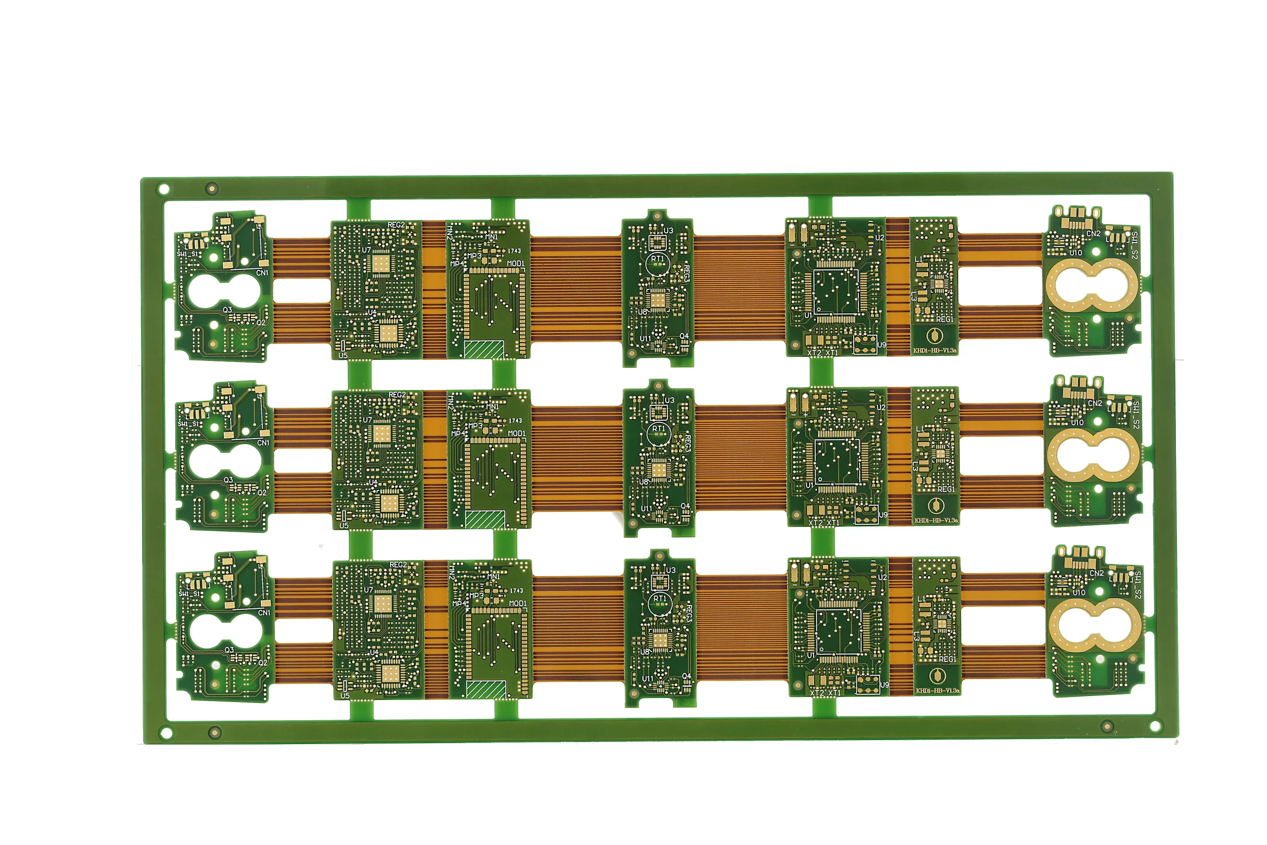


The effect of each approach on PWB manufacturing yields, and thus onboard costs, will be discussed in sequence. It should be noted that the last option is the simplest but the most costly solution, and thus should be used only after the methods suitable for resolving the first two conditions have been proven inadequate for achieving the desirable board density.
The major obstacles preventing the increase of conductor channel capacity are large pad diameters around the plated through-holes (PTHs), since, at the present state of technology, PWBs still require pads wider than the conductors at their location. These pads reduce the obtainable connectivity of PCB boards and must be accounted for in a proper analysis of interconnection density Id. For instance, in one design, the reduction of pad diameters from 55 to 25 mils (by 55 percent) doubled the interconnection density, while the reduction in conductor pitch Cp from 18 to 7 mils (by 61 percent) increased it only by 50 percent.
It is obvious that the reduction of pad diameters, or their total elimination, could be a more efficient way to increase the wiring capacity of complex PWBs. The purpose of copper pads surrounding the drilled holes in PWBs is to accommodate any potential layer-to-layer or pattern-to-hole misregistrations and thus prevent any hole breakout outside the copper area of the pads. This misregistration is caused mainly by the instability and movement of the base laminate during its processing through the PCB or multilayer board (MLB) manufacturing steps
PWB manufacturers are reasonably comfortable with the production of boards with 4- or 5-mil-wide conductors, but they still require large pads around plated holes to ensure against hole breakout. This limits the currently available wiring density to about 40 to 60 in/in2 per Plane. A technology that will permit PCB manufacturers to fabricate invisible vias could increase the connectivity per PWB signal plane from this current range to the level of 100 to 140 in/in2 Conductor widths of 0.002 in will offer a PCB of 200 to 250 in/in2 per signal plane.
The major benefit of such a reduction in the layer count is that it can result in a significant reduction of the manufacturing cost while providing the same total interconnection length.
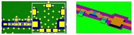
Image 1: The bonding pad on pwb
An obvious method of increasing the connectivity of PWBs is to reduce the widths of conductors and spaces and thus increase the number of available wiring channels on each single plane, as described previously. This is the direction that has been used in the IC and PCB industries for many years. However, it is impossible to decrease conductor widths or spaces indefinitely. The reduction of the conductor width is limited by the current-carrying capacity of thin, small conductors, especially when these conductors are long, as they frequently are on PWBs.
There are processing limits to this conductor reduction, since manufacturing yields may plummet if the reduction stretches the process capabilities beyond their normal limits.There is also a limit to the reduction of the spaces between the conductors, governed mainly by electrical considerations, i.e., by the need to prevent excessive cross-talk, minimize noise, and provide proper signal propagation conditions and characteristic impedance.
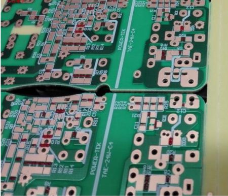
Image 2: The PCB circuit board twisted and deformed during PCBA processing
Still, such conductor reductions, if achieved within the described limits, can be an effective path for increasing the PWB density and the reduction of PCB manufacturing costs. The reduction of conductor widths from 6 to 3 mils halves the number of signal layers necessary to ensure the same connectivity (while their yields, interconnection density, and board area were kept constant). This reduction in the number of layers can significantly reduce the manufacturing costs of PCB boards.
Any successful increase of conductor density Id in PCBs would be effective only if the processes exist that permit manufacture with reasonable yields. Unfortunately, the yields of thin conductors in PWBs fall rapidly as their widths are reduced below 5 mils. Therefore, an understanding of manufacturing yields is very important for analysis of the most cost-effective manufacturing process, because the process yields have a major effect on the cost of interconnection substrates.
Make Your PCB Dreams a Reality with XPCB Limited
XPCB Limited is your go-to partner for turning your PCB dreams into reality. Our streamlined PCB manufacturing process, combined with quick-turnaround prototyping and turnkey PCBA services, ensures that your projects come to life with ease. Trust in our expertise and dedication to quality as we help you achieve your PCB goals. Join us and experience the difference with XPCB Limited.
XPCB Limited is a premium PCB & PCBA manufacturer based in China.
We specialize in multilayer flexible circuits, rigid-flex PCB, HDI PCB, and Rogers PCB.
Quick-turn PCB prototyping is our specialty. Demanding project is our advantage.
Tel : +86-136-3163-3671
Fax : +86-755-2301 2705
Email : [email protected]
© 2023 - XPCB Limited All Right Reserve
