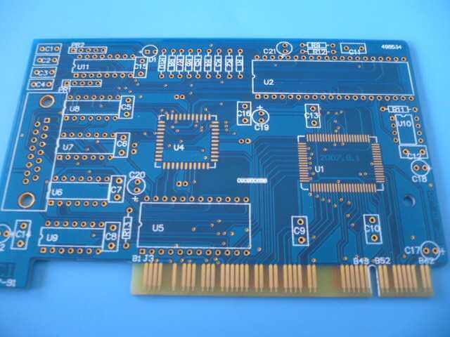
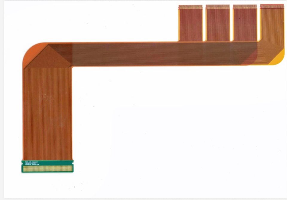
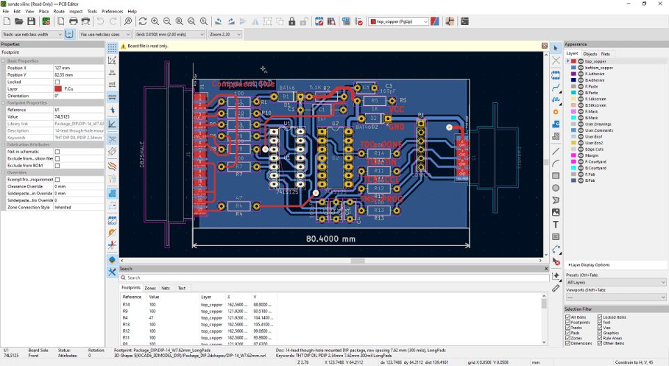
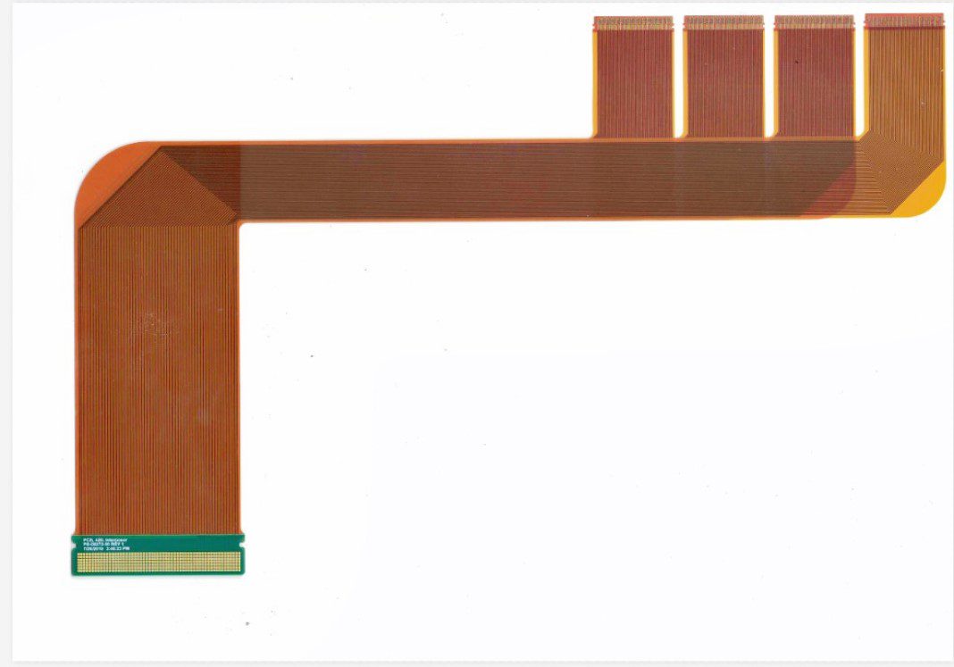
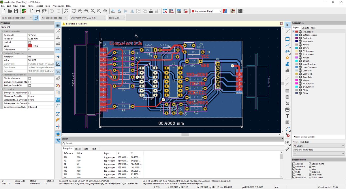
Printed circuit boards have a particularity, that is, each PCB is customized. When we design a project, we are more concerned about layout and wiring, etc., and often ignore which design factors will add additional board manufacturers. Therefore, usually, the original data of the circuit board PCB needs to be sent to the manufacturer to get the correct quotation. Then, what are the design factors of the PCB board that will affect the manufacturing price?
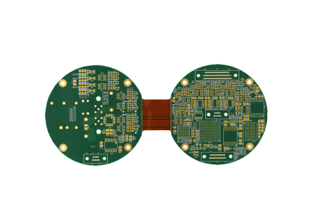
- The number of wiring layers: The more layers of PCB have, the easier the wiring work done. But the price increases linearly with the number of layers, and the final board price may be doubled.
- Vias: If it is not limited by the device PCB or the design density, try to use vias with a diameter above 0.15mm and vias less than 0.15mm. Most PCB manufacturers need to charge a certain processing fee.
- Line width and line spacing: usually less than 3.5mil, the manufacturer will increase the cost.
- Back drilling: use in the backplane or single board with high-speed signals, it will increase the cost by about 10%~20%.
- Holes in the disk: Unless there are restrictions on the signal and layout, the package should not be used.
- HDI and blind buried via design: This item increases the cost of a large proportion if the package allows it, it is best not to use it. Tip: BGA packages with pitch 0.65mm and above can all be fan-out through holes, and some 0.5mm BGA packages can fan-out through holes according to the pad size and available pin distribution.
- Surface technology Immersion gold, Immersion tin, Immersion silver, Gold Finger, the impedance will increase the cost.
- Materials: Unconventional laminate such as high TG material, halogen-free laminate, and high-frequency material will increase the procurement time, which means increased production costs.
The above are the design factors that affect the price of PCB. It is not difficult to find the biggest factors affecting the price of PCB circuit boards, namely the complexity of PCB circuit board proofing depends on the number of layers and vias because this defines the change of layers at which vias start and stop, and more lamination and drilling steps are required in the circuit board manufacturing process.