


PCB factories share 4 common knowledge
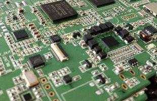
It will produce virtual soldering defects, affect the parameters of the components in the circuit, and lead to the instability of the conduction of the components of the double-layer board. The inner layer causes the failure of the entire circuit function, solderability refers to the nature of the metal surface being wetted by molten solder. That is, the metal surface where the solder is located forms a relatively uniform continuous smooth adhesion film.
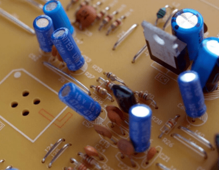
(a) The composition of the solder and the nature of the solder, The Solder is an important part of the soldering chemical treatment process, it is composed of chemical materials containing flux, and the commonly used low melting point eutectic metal is Sn-Pb or Sn-Pb-Ag, in which the impurity content should be controlled by a certain proportion to prevent the oxide generated by impurities from being dissolved by the flux, the function of the flux is to help the solder wet the circuit surface of the soldered plate by transferring heat and removing rust, generally using white rosin and isopropanol solvent.
(b) The soldering temperature and the cleanliness of the metal plate surface will also affect the solderability, if the temperature is too high, the solder diffusion speed will be accelerated, and it has high activity at this time, which will make the PCB and the solder melting surface oxidize rapidly, resulting in soldering defects, and the surface of the PCB will also be polluted to affect the solderability and produce defects, including solder balls, solder balls, open circuits, poor gloss, etc.
Warping of PCBs and components during the welding process, virtual welding, short circuit and other defects due to stress deformation. Warpage is often caused by an unbalanced temperature in the upper and lower parts of the board. For large PCBs, warping can also occur due to the weight of the board itself. The ordinary PBGA device is about 0.5mm away from the PCB, if the device on the PCB is large.
As the PCB cools down and returns to its normal shape, the solder joint will be under stress for a long time, if the device is raised by 0.1mm, it is enough to cause a virtual soldering open circuit;
When the size of the PCB is too large in the layout, although the soldering is easier to control, the printed line is long, the impedance increases, the anti-noise ability decreases, and the cost increases; If it is too small, the heat dissipation will decrease, the soldering is not easy to control, and the adjacent lines are prone to interfere with each other, such as the electromagnetic interference of the PCB, etc., the PCB design must be optimized:
(a) shorten the connection between high-frequency components and reduce EMI interference.
(b) Components with large weight (such as more than 20g) should be fixed with brackets and then welded.
(c) The heat dissipation problem should be considered for the heating element to prevent defects and rework caused by large delta T on the surface of the component, and the thermal element should be kept away from the heat source.
(d) The arrangement of the components is as parallel as possible, so that it is not only beautiful but also easy to weld, and it is suitable for mass production.
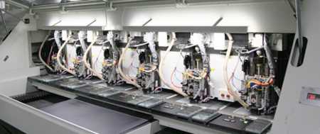
PCB processing process will inevitably encounter several defective products, may be caused by machine error, may also be human reasons, for example, sometimes there will be an abnormal situation called hole breaking state, the cause of the specific situation to be analyzed on a case-by-case basis. If the hole breaking state is a point distribution rather than a whole circle of broken circuits, it is called “point PCB hole breaking” or “wedge PCB hole breaking”. The common cause comes from poor treatment of the slag removal process.
During PCB processing, the slag removal process is first treated with a leavening a
gent, and then the erosion of the strong oxidant “permanganate” is carried out.
Take Your Projects to New Heights with XPCB Limited
XPCB Limited offers top-notch PCB manufacturing, quick-turnaround prototyping, and turnkey PCBA services designed to make your projects shine. Count on us to bring your ideas to life with efficiency and quality. Your success matters to us, and we’re here to make your innovation journey smooth and rewarding.
XPCB Limited is a premium PCB & PCBA manufacturer based in China.
We specialize in multilayer flexible circuits, rigid-flex PCB, HDI PCB, and Rogers PCB.
Quick-turn PCB prototyping is our specialty. Demanding project is our advantage.
Tel : +86-136-3163-3671
Fax : +86-755-2301 2705
Email : [email protected]
© 2023 - XPCB Limited All Right Reserve
