


Packing: All PCBs need to be packed in vacuum bags, with moisture-proof beads inside, and the outer packaging is not allowed to be damaged.
Text printing: the model, version, BOM, and ECN are consistent, the part surface and text, model characters, LOGO, UL, FCC, CE or lead-free marks and other text can not be defective, typo, missing printing, unclear printing and other phenomena.
Surface: PCB surface is not allowed to drill tin in the line, the board surface can not be left solder resist, glue traces, bad labels, etc., copper residue and other non-wire conductors must be more than 2.5mm away from the line, the area must be ≦0.25m㎡, scratch length below 10mm, width below 0.2mm does not hurt the substrate, can not exceed two, non-tinning, gold-plated lines, copper exposure area is not allowed to ≧ 0.5m㎡, green oil wrinkles are not more than 25.4mm, and green oil does not fall, does not affect the solder paste silk screen.
Circuit: PCB line and PAD bit are not allowed to be warped, no line repair is allowed, the line scratch length is less than 5mm, the width is less than 0.2mm, and the copper is not exposed to more than two, and the placement PAD bit of gold finger/CHIP components is not allowed to be repaired.
Flatness: The warpage of the PCB board shall not exceed 8/1000 of the diagonal of the board.
Lamination: no substrate is allowed to have substrate delamination, no cracks are allowed at the edge of the substrate or no PAD holes, the blistering area must be ≧ 0.7mm from the line, and the maximum diameter is not allowed to ≧0.7mm, and it is required to be within the range that the component can cover, the edge of the substrate is ≦ 0.2mm or the uneven burr should be 0.2mm, and there should be no conductor on the board surface and in the surface.
Pad: The trim edge is smooth, clean, and shiny normally, and if the solder joint/pad vaporization color is dirty, it will be rejected.
Size: Measure the size of the puzzle board with the card delay, check the BOM data, and make a timely record of each batch of new circuit incoming circuit or new version of the PCB after the change.
Trimming and drilling: Porous/leaking/inconsistent hole size/plugging holes/hole cracking/oxidation and fouling/affecting weldability, etc. are not allowed.
Gold finger: the cutting edge should be smooth, the surface is clean and not allowed to be stained with green oil, tin, electroplating pores, bubbles, exposed copper, exposed nickel.
Oxidation, obvious discoloration, redness or whitish/black and unclean oil stains, etc., no scratches of exposed copper, each strip shall not exceed 5mm, and each side shall not exceed two.
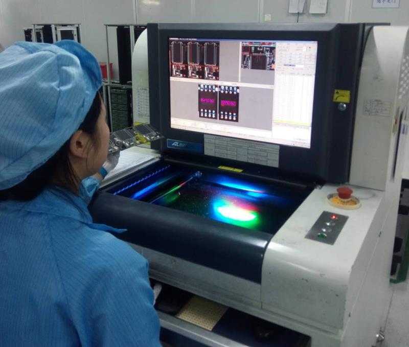
Key checks: Use a microscope to check whether the PCB has oxidation, such as BGA pads and gold fingers.
Multilayer PCB inspection standards for professional PCB manufacturer
The multilayer PCB is made of double-layer boards, the circuit layout is very precise and the components on the board are complex and diverse, how to ensure that these parts meet the specifications, so before the multilayer PCB is manufactured and packaged, it must go through strict testing to ensure that the components on the board meet the specifications and solderability. Testing multilayer PCBs usually uses ICT in-circuit testing or automatic testing machines, using the bed of needles to contact all the test points on the measuring board, what problems do we need to pay attention to during the testing process?
1. PCB zero soldering pad cannot be used as a test point, and a special test pad should be designed. The pads are located on the same side of the multilayer PCB, reducing inspection costs.
2. In order to ensure a secure connection and prolong the service life of the probe, a softer, easily penetrating and non-oxidizing metal should be selected as the probe during the test.
3. The margin of the multilayer PCB at the interval of each test point should be kept at about 5 mm, and the moment between the components should be kept at more than 1 mm to avoid the impact of the probe and components.
4. The diameter of each test point is not less than 0.4mm, and the interval between adjacent test points is about 2.54mm, but not less than 1.27mm.
5. All test points should be evenly distributed on the multilayer PCB to reduce the stress concentration of the probe, and the test breakpoints should be set in different areas of the power cord on the multilayer PCB, so that the power supply can be decoupled or the failure can query the points.
Make Your PCB Dreams a Reality with XPCB Limited
XPCB Limited is your go-to partner for turning your PCB dreams into reality. Our streamlined PCB manufacturing process, combined with quick-turnaround prototyping and turnkey PCBA services, ensures that your projects come to life with ease. Trust in our expertise and dedication to quality as we help you achieve your PCB goals. Join us and experience the difference with XPCB Limited.
XPCB Limited is a premium PCB & PCBA manufacturer based in China.
We specialize in multilayer flexible circuits, rigid-flex PCB, HDI PCB, and Rogers PCB.
Quick-turn PCB prototyping is our specialty. Demanding project is our advantage.
Tel : +86-136-3163-3671
Fax : +86-755-2301 2705
Email : [email protected]
© 2023 - XPCB Limited All Right Reserve
