• +86-755-23012705
  • [email protected]
  • Building 3, Jinfeng Industrial Park, Fuyong Street, Baoan District, Shenzhen ,China
Search
Close
logo
  • Home
  • About Us
    • About XPCB
    • Flexible PCB Fabrication
    • PCB Fab Capability
    • PCBA Capability
    • Our Certifications
    • Our Facility
    • Quality Assurance
  • PCB Fabrication
    • Flexible PCB
    • Rigid Flex PCB
    • Rigid PCB
    • ELIC HDI PCB
    • RF PCB
    • Medical PCB
    • Automotive PCB
    • IoT & IIoT PCB
    • Industrial Control PCB
    • Telecommunication PCB
    • Consumer Electronics PCB
  • PCB Assembly
    • Turn Key PCB Assembly
    • Consigned PCB Assembly
    • Components Sourcing
  • Resources
    • PCB Glossary
    • PCB Design Guide
    • PCB Blog
  • Contact
Menu
  • Home
  • About Us
    • About XPCB
    • Flexible PCB Fabrication
    • PCB Fab Capability
    • PCBA Capability
    • Our Certifications
    • Our Facility
    • Quality Assurance
  • PCB Fabrication
    • Flexible PCB
    • Rigid Flex PCB
    • Rigid PCB
    • ELIC HDI PCB
    • RF PCB
    • Medical PCB
    • Automotive PCB
    • IoT & IIoT PCB
    • Industrial Control PCB
    • Telecommunication PCB
    • Consumer Electronics PCB
  • PCB Assembly
    • Turn Key PCB Assembly
    • Consigned PCB Assembly
    • Components Sourcing
  • Resources
    • PCB Glossary
    • PCB Design Guide
    • PCB Blog
  • Contact
Get Instant Quote

Quality Standard for SMT (2/3)

3、 Criteria for Inspection Standards


3.1 Printing Inspection

General rule: The amount of solder paste printed on the pad is allowed to have a certain deviation, but the area covered by the solder paste on each pad shall be greater than 75% of the pad area.


3.2 Dispensing Inspection

Ideal glue spot: No trace of patch glue contamination can be seen on the pad and lead out end face. The glue spot is located in the middle of each pad, and its size is about 1.5 times that of the dispensing nozzle. The amount of glue is based on the solder end of the component and the PCB after mounting The pads should not occupy dirt.


3.3 Pre Furnace Inspection


3.4 Post Furnace Inspection

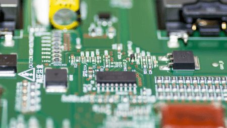
A good solder joint shall be full and well wetted, and the solder shall be spread to the edge of the pad.


4、 Statistics of Quality Defects

In SMT , the statistics of quality defects is very necessary. In the quality defect statistics of reflow welding, we introduce DPM statistical method, that is, the defect statistical method of parts per million. The calculation formula is as follows:

Defect rate [DPM] = total number of defects / total number of solder joints * 106

Total number of solder joints = number of tested circuit boards × Solder joint

Total number of defects = total number of defects detected on the circuit board

For example, if there are 1000 solder joints on a circuit board, the number of detected circuit boards is 500, and the total number of detected defects is 20, it can be calculated according to the above formula:

Defect rate [ppm] = 20 / (1000 * 50) * 106 = 40ppm

5 2 45 20x25 24 Quality Standard for SMT (2/3)


Share

Related posts

2022-05-20

Electromagnetic Compatibility Design of Mobile Phone PCB (1)


Read more
2022-05-20

The PCB Circuit Design of LED Switching Power Supply


Read more
2022-05-20

Electromagnetic Compatibility Design of Mobile Phone PCB (2)


Read more
amazon
amphenol-logo
halliburton
intel logo
samtec logo
sanmina logo
Previous
Next

Company Info

XPCB Limited is a premium PCB & PCBA manufacturer based in China.

We specialize in multilayer flexible circuits, rigid-flex PCB, HDI PCB, and Rogers PCB.

Quick-turn PCB prototyping is our specialty.  Demanding project is our advantage.

Head Office

XPCB Limited
Address :
Building 3, JinFeng Industry Area,  Fuyong Town, Baoan District, Shenzhen, Guangdong, 518103, China.

Tel : +86-136-3163-3671
Fax : +86-755-2301 2705
Email : [email protected]

Quick Links

  • Flexible PCB
  • Rigid Flex PCB
  • ELIC HDI PCB
  • RF PCB
  • PCB Capability
  • PCBA Capabiility
  • About Us

PCB Blog

Electromagnetic Compatibility Design of Mobile Phone PCB (1)

Read More »

The PCB Circuit Design of LED Switching Power Supply

Read More »

Electromagnetic Compatibility Design of Mobile Phone PCB (2)

Read More »

© 2023 - XPCB Limited All Right Reserve