• +86-755-23012705
  • Building 3, Jinfeng Industrial Park, Fuyong Street, Baoan District, Shenzhen ,China
  • [email protected]
logo
  • Home
  • About Us
    • Flexible PCB Expertise
    • Our Certifications
    • Our Facility
    • Quality Assurance
  • PCB Fabrication
    • Flexible PCB
    • Rigid Flex PCB
    • Rigid PCB
    • ELIC HDI PCB
    • RF PCB
    • Medical PCB
    • Automotive PCB
    • IoT & IIoT PCB
    • Industrial Control PCB
    • Telecommunication PCB
    • Consumer Electronics PCB
  • PCB Assembly
    • Turn Key PCB Assembly
    • Consigned PCB Assembly
    • Components Sourcing
  • Capabilities
    • PCB Fab Capability
    • ATE PCB Fabrication
    • PCB Technology Roadmap
    • PCB Assembly Services
    • PCB Design Support
  • Contact
  • Resources
    • PCB Blog
    • PCB Glossary
Get Quote

The Difference Between PCB Through Vias, Blind Vias, And Buried Vias

HDI PCB manufacturer stackup


  • What is a PCB through-hole

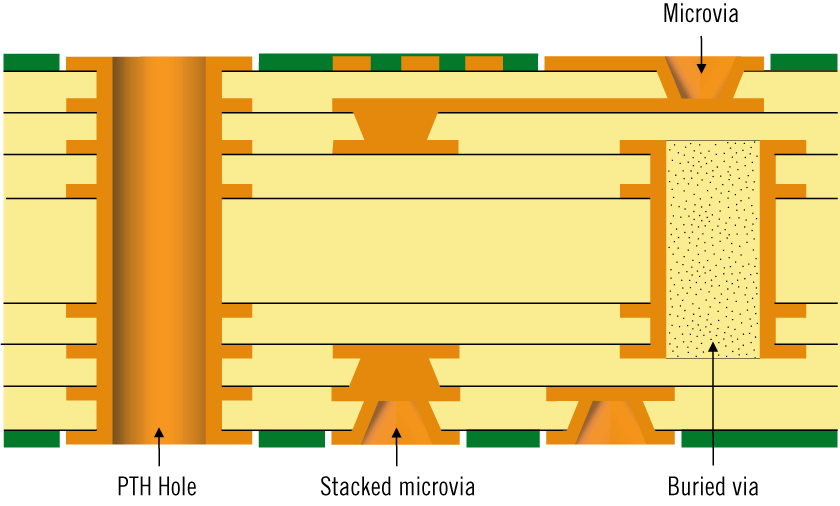
Through-holes are one of the most common types of circuit boards, and the holes that can be seen by simply holding the PCB up to the light are called “through-holes” This is also the simplest kind of hole, because when making it, as long as you use a drill or laser to directly drill the circuit board, the cost is relatively cheap, but relatively, some circuit layers do not need to connect these through holes.

Multi layer PCB stack up The Difference Between PCB Through Vias, Blind Vias, And Buried Vias

For example, we have a six-story house, I bought its third and fourth floors, I want to design a staircase in the interior only connect the third floor and the fourth floor, for me the space on the fourth floor is virtually connected to the first floor to the sixth floor of the stairs to use up some more space.


  • What is a PCB blind via

In order to increase the space utilization of the PCB circuit layer, the “blind hole” process came into being, and the production method needs to pay special attention to the depth of the drilling hole (Z-axis) to be just right. But this method often causes the difficulty of electroplating in the hole, so it is almost adopted by no manufacturer.

HDI stackup


It is also possible to drill holes in advance for the circuit layers that need to be connected in individual circuit layers and then glue them together which requires more precise positioning and alignment devices.


  • What is PCB Via Buried

The connection of any circuit layer inside the PCB board but not connected to the outer layer, the process can not be achieved by drilling after bonding. It must be drilled at the time of individual circuit layers, first partially glued to the inner layer and then electroplated first, and finally all bonded.

The production process is more labor-intensive than the previous two, so the manufacturing price is also the most expensive. This process is usually only used in high-density (HDI) circuit boards, to increase the usable space of other circuit layers.


Flexible pcb manufacturer


Take Your Projects to New Heights with XPCB Limited
XPCB Limited offers top-notch PCB manufacturing, quick-turnaround prototyping, and turnkey PCBA services designed to make your projects shine. Count on us to bring your ideas to life with efficiency and quality. Your success matters to us, and we’re here to make your innovation journey smooth and rewarding.
Share

Related posts

dispensing in PCB
2025-02-07

Multilayer PCB Assembly and HDI PCB Manufacturing for High-Tech Solutions


Read more
smt product line
2025-02-06

Streamline Your PCB Production with XPCB’s Turnkey PCBA Services


Read more
2025-02-05

Comprehensive Turnkey PCBA Services: From BOM to SMT Assembly


Read more
amazon
amphenol-logo
halliburton
intel logo
samtec logo
sanmina logo

Company Info

XPCB Limited is a premium PCB & PCBA manufacturer based in China.

We specialize in multilayer flexible circuits, rigid-flex PCB, HDI PCB, and Rogers PCB.

Quick-turn PCB prototyping is our specialty.  Demanding project is our advantage.

Head Office

XPCB Limited
Address :
Building 3, JinFeng Industry Area,  Fuyong Town, Baoan District, Shenzhen, Guangdong, 518103, China.

Tel : +86-136-3163-3671
Fax : +86-755-2301 2705
Email : [email protected]

Quick Links

  • Flexible PCB
  • Rigid Flex PCB
  • ELIC HDI PCB
  • RF PCB
  • PCB Capability
  • PCBA Capabiility
  • About Us

PCB Blog

Multilayer PCB Assembly and HDI PCB Manufacturing for High-Tech Solutions

Read More »

Streamline Your PCB Production with XPCB’s Turnkey PCBA Services

Read More »

Comprehensive Turnkey PCBA Services: From BOM to SMT Assembly

Read More »

© 2024 - XPCB Limited All Right Reserve