


The initial stage of the wave soldering process in the PCBA package is the most crucial part of the entire wave soldering quality control link, as long as this part of the preparation work carefully done, we only use the rest of the production process of temperature control, transmission speed and inclination control will be able to ensure the quality of the PCBA package wave soldering.
The Wave Soldering Process of Single Machine Type
First, component lead forming a printed board paste solder resist tape; second, inserted components; third, printed board into the welding fixture; fourth, coated flux; fifth, preheating; sixth, wave soldering; seventh, cooling; eighth, remove the printed board; ninth, tear off the solder resist tape; tenth, inspection; eleventh, Xin L welding; twelveth, cleaning; thirteenth, inspection; fourteenth, into the transport box.
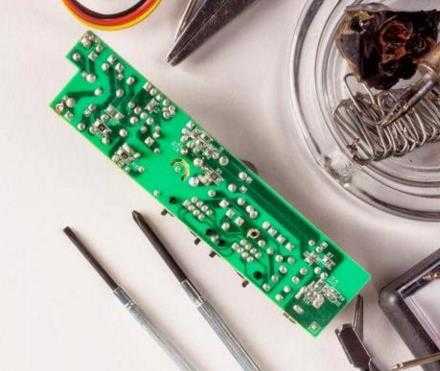
The Initial Phase of Wave Welding for PCBA Package
1, Drying in the manufacturing process of PCBA may contain residual solvents and moisture, if there are bubbles on the PCB in the welding process to produce the phenomenon, it is best to PCB pre-drying process before the line. 1.5mm or less thin PCBA can choose a lower temperature and shorter time, multi-layer PCB can be in 105 degrees Celsius continuous drying two to four hours. PCB pre-drying Drying can effectively eliminate the residual stress formed in the PCBA board making process, but also to reduce the PCB warpage and deformation of wave soldering phenomenon.
2, Preheating preheating temperature is not fixed, but with the time, power supply voltage, ambient temperature, season and ventilation and other factors to adjust the change.
3, The solder we need to melt should be with good fluidity and wettability, and in this case the soldering temperature should be higher than the melting point of the solder itself.
4, Transmission PCBA package in the welding time and transmission speed is closely related. We can determine the best transmission speed we need in wave soldering according to the specific production efficiency, the thermal capacity of PCB substrate and components, preheating temperature and other factors.
5, Inclination angle transmission inclination angle is now the most widely used in the PCBA package industry is 4 ° ~ 6 °. This range can effectively reduce the lack of tin, less tin, even tin and other undesirable phenomena.
XPCB Limited is a premium PCB & PCBA manufacturer based in China.
We specialize in multilayer flexible circuits, rigid-flex PCB, HDI PCB, and Rogers PCB.
Quick-turn PCB prototyping is our specialty. Demanding project is our advantage.
Tel : +86-136-3163-3671
Fax : +86-755-2301 2705
Email : [email protected]
© 2023 - XPCB Limited All Right Reserve
