• +86-755-23012705
  • Building 3, Jinfeng Industrial Park, Fuyong Street, Baoan District, Shenzhen ,China
  • [email protected]
logo
  • Home
  • About Us
    • Flexible PCB Expertise
    • Our Certifications
    • Our Facility
    • Quality Assurance
  • PCB Fabrication
    • Flexible PCB
    • Rigid Flex PCB
    • Rigid PCB
    • ELIC HDI PCB
    • RF PCB
    • Medical PCB
    • Automotive PCB
    • IoT & IIoT PCB
    • Industrial Control PCB
    • Telecommunication PCB
    • Consumer Electronics PCB
  • PCB Assembly
    • Turn Key PCB Assembly
    • Consigned PCB Assembly
    • Components Sourcing
  • Capabilities
    • PCB Fab Capability
    • ATE PCB Fabrication
    • PCB Technology Roadmap
    • PCB Assembly Services
    • PCB Design Support
  • Contact
  • Resources
    • PCB Blog
    • PCB Glossary
Get Quote

16-layer Rigid PCB Manufacturer Analyzes The Aauses Of Warpage On Rigid PCBs

1 4 16-layer Rigid PCB Manufacturer Analyzes The Aauses Of Warpage On Rigid PCBs


There are two key points to prevent warpage of 16-layer rigid PCB


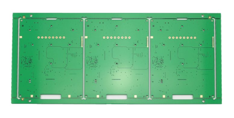
The two main reasons for the warping of rigid PCB are: 1. The substrate storage method is incorrect, 2. The improper production operation causes the warping, for these two problems, it is still possible to avoid them as long as you observe carefully, this chapter mainly focuses on the problem of warping of rigid PCBs to do a detailed explanation!

Storage: Because the copper-clad laminate will increase warpage due to moisture absorption during storage, the single-sided copper-clad laminate has a large moisture-absorbing area. If the inventory environment humidity is high, the single-sided copper-clad laminate will greatly increase the warpage. The moisture of the double-sided copper-clad laminate can only penetrate from the end face of the product, the moisture absorption area is small, and the warpage changes slowly.

For copper-clad laminates without moisture-proof packaging, attention should be paid to warehouse conditions to minimize humidity in the warehouse and to avoid exposed copper-clad laminates to avoid warping of copper-clad laminates during storage. Improper placement of copper-clad laminates will increase warpage, vertical placement on copper-clad laminates or heavy objects, poor placement, etc. will increase the warpage of copper-clad laminates.


16-layer rigid PCB


For PCB rigid boards, it is also necessary to pay attention to the anti-interference ability of the whole board, and the conventional methods are:

  1. Add a filter capacitor near the power supply and ground of each IC, typically with a capacity of 473 or 104;
  2. For sensitive signals on the printed PCB, the included shielded wires should be added separately and the wiring near the signal source should be as little as possible;
  3. Choose a reasonable grounding point.


What are the ways to test the temperature profile of a 16-layer rigid PCB?


Since the printed solder paste does not solder the PCB assembly board and cannot fix the electrical test end of the thermocouple, it is necessary to use the actual soldered product for testing. The test temperature does not exceed the limit temperature, and the assembled board can be used as a formal product after testing 1 to 2 times (the test board cannot be used repeatedly and more than 2 times). After long-term high-temperature welding, the color of the multi-layer board will change from light to dark or yellowish-brown.

Although the heating method of the all-hot blast stove is mainly convective conduction, there is also a small amount of radiation conduction. Dark brown absorbs more heat than a regular light green PCB, so the measured temperature will also be slightly higher than the actual temperature.


16-layer rigid PCB


So how to quickly test the temperature curve of 16-layer rigid PCB, and what are the specific methods and steps?

  1. According to the complexity of the multi-layer PCB assembly and the number of channels of the collector, more than three test points are selected as the test points, which can reflect the representative temperature test points of high (hot spot), medium and low (cold spot) on the surface assembly of the16-layer rigid PCB.
  2. Remove the solder on the multi-layer PCB solder joint, and use high-temperature solder (Sn-90Pb, solder with a melting point of more than 289 °C) to solder the test ends of multiple thermocouples on the test points respectively, or use high-temperature tape paper to glue the test ends of the thermocouples to each temperature test point of the multi-layer PCB.
  3. Insert the other end of the thermocouple into the 1.2.3…. position, and do a good job of each thermocouple number and the corresponding position on the surface assembly plate.
  4. The multi-layer PCBassembly board on the surface to be tested is placed on the conveyor chain/mesh belt at the entrance of the reflow soldering machine, and the KIC temperature curve test program is started, and the real-time curve is marked on the screen with the movement of the multi-layer PCB.
  5. After the multi-layer PCB is cooled down, pull the thermocouple wire and drag the PCB assembly board back, and when the complete temperature curve and peak temperature/schedule are displayed on the screen, it means that the test link has been completed.


16-layer rigid PCB


Your Trusted Partner for PCB Success: XPCB Limited
Let XPCB Limited be your guide to PCB success. Our comprehensive PCB manufacturing, rapid prototyping, and turnkey PCBA services are designed to meet your needs with ease. Count on us to deliver reliable solutions that exceed your expectations. With XPCB Limited, your journey to PCB excellence starts here.
Share

Related posts

dispensing in PCB
2025-02-07

Multilayer PCB Assembly and HDI PCB Manufacturing for High-Tech Solutions


Read more
smt product line
2025-02-06

Streamline Your PCB Production with XPCB’s Turnkey PCBA Services


Read more
2025-02-05

Comprehensive Turnkey PCBA Services: From BOM to SMT Assembly


Read more
amazon
amphenol-logo
halliburton
intel logo
samtec logo
sanmina logo

Company Info

XPCB Limited is a premium PCB & PCBA manufacturer based in China.

We specialize in multilayer flexible circuits, rigid-flex PCB, HDI PCB, and Rogers PCB.

Quick-turn PCB prototyping is our specialty.  Demanding project is our advantage.

Head Office

XPCB Limited
Address :
Building 3, JinFeng Industry Area,  Fuyong Town, Baoan District, Shenzhen, Guangdong, 518103, China.

Tel : +86-136-3163-3671
Fax : +86-755-2301 2705
Email : [email protected]

Quick Links

  • Flexible PCB
  • Rigid Flex PCB
  • ELIC HDI PCB
  • RF PCB
  • PCB Capability
  • PCBA Capabiility
  • About Us

PCB Blog

Multilayer PCB Assembly and HDI PCB Manufacturing for High-Tech Solutions

Read More »

Streamline Your PCB Production with XPCB’s Turnkey PCBA Services

Read More »

Comprehensive Turnkey PCBA Services: From BOM to SMT Assembly

Read More »

© 2024 - XPCB Limited All Right Reserve