


What are the common PCB surface treatment processes: tin spraying (lead-free tin spraying or leaded tin) / hot air leveling, organic coating, chemical gold, electroplating nickel gold, immersion silver, immersion tin, carbon oil, halogen-free gold finger, OSP anti-oxidation, etc.;
As far as lead and lead-free are concerned, as more and more attention is paid to the environmental protection issues involved in the production process of printed circuit boards, the lead-sprayed tin process is decreasing, and more and more enterprises choose lead-free tin spraying process, and all printed circuit board companies must meet the requirements of ROHS environmental protection, otherwise for some long-term products of enterprises, even the most basic audit can not be passed, not to mention that they want to have a cooperative relationship with them.
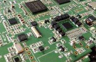
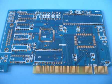
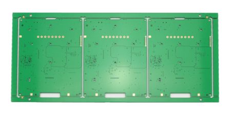
The surface treatment process technology of printed circuit board refers to the surface treatment process method of artificially forming a layer on PCB components and electrical connection points that is different from the mechanical/physical and chemical properties of the substrate. The function of PCB surface treatment is to confirm that the product has good solderability and electrical properties, and the direct exposure of copper will make it easy to oxidize, and the PCB board must go through the surface treatment process when producing circuit boards, no matter what field it is used in.
Here’s what the definition of each PCB surface treatment process is!
Tin spraying process is also known as “hot air leveling”, the surface of the PCB is coated with molten tin and lead solder and leveled (blown flat) with heated compressed air to form a coating layer that is resistant to copper oxidation and can provide good solderability, and the solder and copper form a copper-tin metal compound at the junction when hot air leveling, with a thickness of about 1~2mil. The PCB is immersed in molten solder during the tin spraying process, and the air knife blows the liquid solder before the solder solidifies, and can minimize the meniscus of the solder on the copper surface and prevent solder bridging.
It is generally believed that the horizontal type is better, mainly because the horizontal hot air leveling coating is relatively uniform, and automatic production can be realized. The general process is as follows: micro-etching – > preheating – > coating flux – > tin spraying – > cleaning.
The OSP process is also known as “organic coating”, the difference between the OSP antioxidant process and other processes is that the OSP antioxidant process acts as a barrier layer between copper and air, which can be simply understood as OSP is to grow an organic film on a clean bare copper surface by chemical methods. This film has good oxidation/thermal shock/moisture resistance to protect the copper surface from rusting (oxidation or vulcanization) in the normal environment, and must be easily removed by the flux during the subsequent soldering high temperatures for soldering.
The OSP oxidation resistance process is simple to make and relatively affordable in cost, so it is widely used. To ensure that multiple reflow soldering can be performed, the copper surface needs to have multiple layers of organic coating, and only one organic coating layer is not possible, which is why it is often necessary to add molten copper to the chemical tank. After the first layer of PCB board is coated, the coating layer adsorbs copper, and then the organic coating molecules of the second layer combine with copper, and even more hundreds of organic coating molecules need to be gathered on the copper surface.
Process flow: degreasing – > micro-etching – > pickling – > pure water cleaning – > organic coating – > cleaning, process control is relatively easy compared with other treatments.
Chemical gold process, also known as “electroless nickel plating/immersion gold”, refers to the copper surface of the PCB wrapped with a thick layer of gold, and the nickel-gold alloy with good electrical properties can extend the protection period of the PCB board. The advantage of chemical gold compared to the OSP process is that it is not only treated with an anti-rust barrier layer, but also can be useful and achieve good electrical properties during the long-term use of the PCB.
The gold process is also very tolerant to the environment, and the electroless nickel coating process will diffuse between gold and copper, and the nickel layer can prevent the diffusion between them, and if the nickel layer is not blocked, the gold will diffuse into the copper within a few hours.Another benefit of electroless nickel/immersion gold plating is the strength of nickel, only 5um thickness of nickel can control the expansion in the Z direction at high temperatures, electroless nickel plating/immersion gold can also prevent the dissolution of copper, which is more beneficial for lead-free soldering.
Chemical gold manufacturing process: depickling and cleaning–> micro-etching–> pre-preg>–activation–> electroless nickel plating–> chemical immersion gold; there are 6 chemical tanks in the process, involving nearly 100 kinds of chemicals, and the process is relatively complex.
Immersion Silver Process: Between OSP and electroless nickel/immersion gold, the immersion silver PCB process is simpler/faster. Immersion silver eliminates the need to put a thick layer of armor on the PCB, providing good electrical properties and maintaining good solderability even when exposed to heat, humidity and pollution. Cons: Tarnishing. There is no nickel underneath the silver layer, and immersion silver does not have all the good physical strength of electroless nickel/immersion gold.
Silver immersion is a displacement reaction, which is almost sub-micron coated with pure silver, and the silver immersion process also contains some organic matter to prevent silver corrosion and eliminate silver migration problems. It is generally difficult to measure this thin layer of organic matter, and analysis has shown that the weight of the organism is less than 1%.
What are the tin immersion processes for the surface treatment process of printed circuit boards: all solder is tin-based, and the tin layer can be matched with any type of solder, and the most primitive PCB is prone to tin whiskers after the tin immersion process. The use of the tin immersion process was limited by the reliability issues of tin whisker and tin migration during the soldering process, and organic additives were added to the tin immersion solution to give the tin layer structure a granular structure.
It not only overcomes the shortcomings of the original immersion tin, but also has good thermal stability and solderability. The immersion tin process can form a flat copper-tin intermetallic compound, so that the immersion tin has the same good solderability as hot air leveling without the headache of flatness of hot air leveling, and there is no diffusion problem between electroless nickel plating/gold immersion metals, but the immersion tin plate can not be stored for too long.
Electroplating nickel gold process: the conductor on the surface of the PCB is electroplated with a layer of nickel and then plated with a layer of gold, nickel plating is mainly to prevent the diffusion between gold and copper, electroplated nickel gold is divided into “soft gold” (pure gold/gold surface does not look bright) and “hard gold plating” two kinds (the surface is smooth and hard, wear-resistant, containing cobalt and other elements, and the surface looks brighter).
Soft gold is mainly used for gold wire in chip packaging, and hard gold is mainly used in the electrical interconnection (such as gold finger) at the non-soldering place, soldering will cause the electroplated gold to become brittle, which is undoubtedly shortening the service life of the PCB board, so it is necessary to avoid soldering on the electroplated gold. However, electroless nickel/immersion gold is brittle because the gold is very thin and consistent.
Electroless palladium plating process: The process is roughly the same as that of electroless nickel plating. Palladium ions are reduced to palladium on the catalytic surface by reducing agents (such as sodium hypophosphite monohydrochloride), and the nascent palladium can be called a catalyst to promote the reaction, so that a palladium plating layer of any thickness can be obtained. The advantages of electroless palladium plating are good welding reliability/thermal stability/surface flatness, and the disadvantage is that palladium is a relatively rare precious metal, so there is also a reason for the increase in production costs.
Your Trusted Partner for PCB Success: XPCB Limited
Let XPCB Limited be your guide to PCB success. Our comprehensive PCB manufacturing, rapid prototyping, and turnkey PCBA services are designed to meet your needs with ease. Count on us to deliver reliable solutions that exceed your expectations. With XPCB Limited, your journey to PCB excellence starts here.
XPCB Limited is a premium PCB & PCBA manufacturer based in China.
We specialize in multilayer flexible circuits, rigid-flex PCB, HDI PCB, and Rogers PCB.
Quick-turn PCB prototyping is our specialty. Demanding project is our advantage.
Tel : +86-136-3163-3671
Fax : +86-755-2301 2705
Email : [email protected]
© 2023 - XPCB Limited All Right Reserve
