- +86-755-23012705
- Building 3, Jinfeng Industrial Park, Fuyong Street, Baoan District, Shenzhen ,China
- [email protected]

The following is the detailed production method and matters needing attention:
I. Original manuscript (using film or sulphate paper)
The designed circuit diagram is printed with a laser (inkjet) printer on transparent film or translucent sulphate paper.
Matters needing attention
The exposed part will be removed by the developer to reveal the copper surface. In addition, mirror printing should be selected when printing the original manuscript. The circuit diagram printing ink (toner) surface must be closely connected with the green photosensitive film surface to obtain the highest resolution.(Drawing software has the function of Mirror printing)
2. If there are holes in the circuit, please repair them with oily black pen.
3. The draft surface should be kept clean and free of dirt.

Second, the exposure
First, tear off the protective film, paste the printing surface of the printed circuit diagram (toner surface/ink surface) on the photosensitive film surface, and then press the manuscript and the photosensitive plate with glass, the tighter the resolution is the better.
A: Standard exposure time with 20W daylight lamp: 8-10 min/min (transparent draft)13-15 min (translucent)
B: Using sunlight: Standard time:
Strong daylight transparent draft takes 1-2 minutes (translucent draft takes 2-4 minutes)
Low sunlight transparent draft takes 2-3 minutes (translucent draft takes 4-5 minutes)
Double panel exposure method:
1. The preferred method of hole positioning for double panel exposure: double face of the original manuscript, fixed with adhesive paper, well matched and fixed with the photosensitive plate without the protective film removed, and diagonally drilled positioning holes with a small 1.0mm drill.Finally, align the positions with the help of two small bits, fix them with adhesive paper, and then expose them separately.
2. Another method: the manuscript is double-faced, fixed on both sides with adhesive paper, and then inserted into the photosensitive plate.Double-sided adhesive paper is used to paste and fix the original manuscript with the photosensitive plate.

Fine lines less than 0.5mm must be double-sided exposure machine.
Third, imaging
1. Modulate imaging agent: Imaging agent: water (1:80), that is, 1 pack of 20g imaging agent and 1600 ml of water can develop about 8 10x15cm single photosensitive plates (mineral water bottle is generally marked with capacity, reference, please use plastic basin instead of metal basin for imaging)
2. Development: Put the photosensitive plate facing up (double panel must be suspended)
Shake the container or plate every few seconds until the copper foil is clear and no longer fogs green.Wait a few seconds to make sure the image is 100% complete.
* Standard operation development time is about 1-2 minutes, development can be carried out in the general light, the most critical is to pay attention to the development progress at any time, never copy the development time.
3. Water:
4. Drying and inspection: In order to ensure that there is no damage to the film surface, it is better to do this step.Blow dry with a hair dryer, scrape the short circuit with a knife, and repair the broken wire with an oily pen.
Matters needing attention
1. Use mineral water bottle to modulate the development liquid in proportion first. It can be poured out for use at any time, but the used development liquid cannot be poured back into the bottle.
2. The thicker the development fluid is, the faster the development speed will be, but too fast will cause the development to be excessive (the line will be blurred and shrunk in all directions).Too thin, the development is slow, easy to cause the development of insufficient (eventually resulting in incomplete etching).
3. Do not pour back the used development fluid.The used development fluid will gradually decompose by itself after 24 hours without causing environmental pollution.
4. Strictly prevent scratch film surface.
Four, etching
Preparation of ferric chloride etching solution :250g ferric chloride is prepared with 1500ml – 2000ml water, which can be melted with hot water as far as possible to avoid etching fine lines.
A. Plastic basin: etching time is about 5 ~ 15 minutes. Shake the plastic basin gently when etching.
B. Etching machine: Etching time with etching machine – new liquid takes about 1.5 ~ 3 minutes.Thin lines less than 0.5mm must be etched.
C. wash:
D. drying:
Matters needing attention
1. Be careful not to injure the membrane surface.
2. Put the plate into the etching solution for about 2 seconds and then take it out for inspection to check the success of the development results.
Remedy for underdevelopment: pick up the plate from the etching solution, and the copper foil strain in the non-circuit part is pink. If the strain is unchanged in some places, then the underdevelopment is indicated.The remedy is to rinse the product with water before redeveloping it in the development solution and then examine it (the development time should be reduced appropriately).
3. Photosensitive film can be directly welded without removal, if necessary to remove available alcohol, acetone and other solvents.
4. The thicker the etching solution is, the slower it will be.
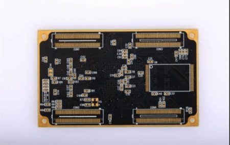
The figure below shows the schematic board made
Plate making the fact is very simple, give to all of the above time is only a reference, the key is your own actual testing, the grasp of the best way is to use the time for a few small plate to test, generally one or two can have a good command, again after mastering the real production, in order to avoid waste.And after you become skilled, the effect of the circuit board you randomly produce will not be worse than that of the professional PCB manufacturer, no matter it is exquisite or professional.
———————————————————————————————————-
Photosensitive plate for the majority of electronic enthusiasts, electronic professional students, electronic research and development and testing industry engineers and technicians to provide convenient production.It can be made by users in a short time without professional production equipment.(Please refer to the instruction for the production method).
Standard size: 100mm × 150mm single-sided electric board.Photosensitive film uniform, fast exposure, easy to judge the result of development, high success rate, easy to use, low cost, strong confidentiality.10 yuan per tablet, 1 package of developer, 10 yuan in total.(One pack of developer allows five standard 100mm × 150mm plates to be imaged!)Good batch price.
Photosensitive circuit board is also called photosensitive circuit board, is through direct irradiation evenly coated in the circuit board photosensitive film, there is light where the film will be dissolved by the developer, there is no solution of the photosensitive film is retained in the circuit board copper skin, do not let ferric chloride solution corrosion, finally retained as a line!
High precision base circuit board can be corroded by special corroders of 0.2mm/0.1mm (equivalent to three lines within 1mm), and the lines of 0.3mm/0.2mm (equivalent to two lines within 1mm) can also be corroded under amateur conditions. However, it is very difficult to walk a line within 1mm (i.e., the width and spacing of the lines are 0.6mm/0.4mm respectively) if the lines are generally depicted by hand.
Above is the actual situation, the accuracy has been very high, than the computer motherboard, memory on the line accuracy is also high.As for, some people say that higher accuracy can be achieved by mechanical methods, that is a lie, it is possible to spend a long time to make a little bit of a demonstration of the small sample, it is not really used.(Even for computer engraving, it is difficult to buy a 0.2mm milling cutter.)
In short, no process can match the precision of printed circuit boards, otherwise the science of the world would have to be completely rewritten.
However, in the case of amateur, due to the limitations of all aspects (no corrosion machine, no exposure machine, no experience), generally can also be made by hand easily 0.4mm / 0.2mm circuit board, basically do not need any processing and modification!The station master has made a 0.3mm/0.2mm circuit board with plain white paper, photosensitive plate, developer, ferric chloride.
Production experience:
1, if the use of film film for exposure, exposure time a little longer does not matter, the most important is that the film should be close to the photosensitive film, do not let the film be exposed.
(Because the contrast between light and non-light is the most important thing a film needs, the film circuit can effectively block light.)
2, if use translucent paper, vegetable parchment do sketches to exposure, time is important, because the part line needs a longer exposure time, and the imagery line of resistance performance and light is not very good (depending on the draft paper smoothness and of sharpness, contrast), if the printer toner, ink cartridges cut water, don’t use such as sketches.
3, if the exposure is severely excessive (more than one time normal), then the development will be very fast, a few seconds to ten seconds can be completed, a little longer time will be completely dissolved in the film, the production failure.
4, if the exposure is seriously insufficient (less than half of the normal), then the development will be very slow, even take a few minutes to complete, at this time must be patient, do not go to repeat the exposure, otherwise the production must fail.
5. Finally, the concentration of the developer is also closely related to its affluence.Concentration is generally prepared by a pack of 10 grams with 1000 milliliters of water, if the developer less, will develop to the midway will become very slow or stop the development, resulting in photosensitive film can not be dissolved, the time is too long will be produced failure.The remedy is to continue developing immediately with the new drug water.
(This problem is often to save material, material and use, small area of the board with a small volume of developer, the results are not worth the cost.)
In short, on the experience of the webmaster, the normal production, the success rate is close to 100 percent, basically do not need any repair.More times, occasionally there will be one or two drift (forgot to look at the time.Webmaster with the sun exposure, but the cloudy day, it will wait for more, the results forget the time) and failure.However, failure is also a gain, that is, to get a bare copper circuit board without corrosion, but also have a few dollars left!
It is recommended that beginners will first board into six, each small board 50mm*50mm (do not look at this small board, it can be loaded with a lot of components), you can do 6 tests, summarize the experience of 6 times, soon you can also guarantee 100 percent success!(This site has made a new wireless microphone of a small circuit board. Each board is only 18mm*24mm, which is several times smaller than 50mm*50mm.)
Note: blasting time, long point short point does not matter much, the main thing is that the place should be blasted light must be enough light, should not be blasted light where the Lord do not explode light (the stationmaster estimate using film and blasting machine, it does not matter if the blasting time is several times longer, it is suggested that the blasting time as long as possible.).Build your own experience.The usage is exactly the same


XPCB Limited is a premium PCB & PCBA manufacturer based in China.
We specialize in multilayer flexible circuits, rigid-flex PCB, HDI PCB, and Rogers PCB.
Quick-turn PCB prototyping is our specialty. Demanding project is our advantage.
Tel : +86-136-3163-3671
Fax : +86-755-2301 2705
Email : [email protected]
© 2024 - XPCB Limited All Right Reserve
