


There are single-sided, double-sided and multilayer PCB. For simple electrical appliances such as radios, single-sided PCBs can be used. However, with the progress of the times, electronic products need to be updated no matter whether it is function or volume. For multi-functional, small-volume electronic products, single-sided and double-sided PCB cannot fully meet the requirements, and multilayer PCBs must be used.
Multi-layer PCB has many advantages, such as high assembly density, small size, shortened wiring between electronic components, fast signal transmission speed, convenient wiring, good shielding effect, and so on. The number of layers of multilayer boards is not limited. There are currently more than 100 layers of PCBs, and the common ones are four-layer and six-layer boards.
When designing a multi-layer board, the layers should be symmetrical, and it is best to have an even-numbered copper layer. If it is asymmetrical, it is easy to cause distortion. Multi-layer board wiring is carried out according to circuit functions. When wiring on the outer layer, more wiring is required on the soldering surface and less wiring on the component surface, which is conducive to the maintenance and troubleshooting of the printed board. In terms of wiring, it is necessary to separate the power layer, ground layer, and signal layer to reduce interference between power, ground, and signals. The lines of two adjacent layers of printed boards should be as perpendicular to each other as possible, or follow diagonal lines or curves, and not parallel lines, so as to reduce the coupling and interference between the substrate layers.
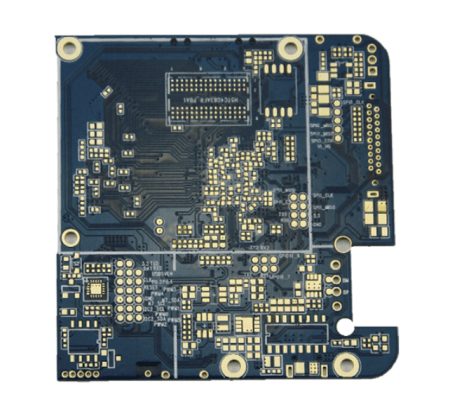
Compared with single-sided and double-sided multi-layer PCB, which layers are composed of? What does each layer represent and what is the use? Multi-layer PCB is mainly composed of the following layers: Signal Layers, InternalPlanes, Mechanical Layers, Masks, Silkscreen, and System.
The signal layer is divided into top layer, middle layer, and bottom layer, which are mainly used for placing various components, or for wiring and soldering. The internal power layer is also called the internal power layer, dedicated to the arrangement of power lines and ground wires. The mechanical layer is generally used to place indicative information about board manufacturing and assembly methods, such as circuit board physical size lines, data information, and via information. The solder mask layer also has a top layer and a bottom layer, and the pads or other objects placed on this layer are copper-free areas. The silk screen layer is mainly used to draw the outline of the component, the number of the placed component or other text information, and the system working layer is used to display information that violates the design rule inspection.
XPCB Limited is a manufacturer specializing in the production of high-precision double-sided, multi-layer and impedance, blind buried vias, and thick copper circuit boards. The products cover HDI, thick copper, backplanes, rigid-flex combined, buried capacitance and buried resistance, Golden Finger and other types of circuit boards, which can meet the needs of customers for various products.
XPCB Limited is a premium PCB & PCBA manufacturer based in China.
We specialize in multilayer flexible circuits, rigid-flex PCB, HDI PCB, and Rogers PCB.
Quick-turn PCB prototyping is our specialty. Demanding project is our advantage.
Tel : +86-136-3163-3671
Fax : +86-755-2301 2705
Email : [email protected]
© 2023 - XPCB Limited All Right Reserve
