


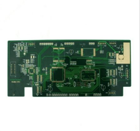
HDI circuit board is defined as a printed circuit board with an aperture of less than 6mil(0.15mm), a HolePad of less than 0.25mm, a contact density of more than 130 points/square inch, a wiring density of more than 117 “/ square inch, and a line width/spacing of less than 3mil/3mil.Generally speaking, HDI circuit board has the following advantages:
1. It can reduce THE COST of PCB: when the DENSITY of PCB increases by more than eight layers, IT can be manufactured with HDI Compared with the traditional pressing method reduced the cost .
2. It Increase line density: The interconnection between traditional circuit boards and components must be connected by the lines leading around the QFP and the through-hole conductor (fan-in and fan-out), so these are the line needs to take up some space.The microporous technology can hide the wiring needed for interconnection to the next layer, and the connection between the mat and the lead between different layers can be directly connected by the blind hole inside the mat, without the need for fan-in and fan-out wiring.Therefore, some pads (such as mini-BGA or CSP ball welding) can be placed on the outer panel surface to undertake more parts, which can increase the density of the circuit board.This new method of stack and wiring is used in the cell phone boards of many high-powered small wireless phones.
3. Conducive to the use of advanced construction technology: conventional drilling technology cannot meet the needs of small parts for the new generation of fine lines due to the size of welding pad (through hole) and mechanical drilling problems.With the development of microporous technology, designers can integrate the latest high-density IC construction technologies, such as matrix package, CSP and DCA into the system.
4,There has a better performance and accuracy of the signal: using microporous interconnections in addition can reduce the signal reflection and the lines between the string of interference, and makes the design of the circuit board line can add more space, is due to the structure and physical properties of microporous hole small and short, so can reduce the inductance and capacitance effect, also can reduce the switching noise signal.
5. Better reliability: Micropores have a thinner thickness and a 1:1 aspect ratio, so the signal transmission reliability is higher than ordinary through-holes.6. Thermal properties can be improved: Insulating dielectric materials of HDI plates have higher glass conversion temperature (Tg), so they have better thermal properties.
6. Thermal properties can be improved: Insulating dielectric materials of HDI plates have higher glass conversion temperature (Tg), so they have better thermal properties.
7. Improved RF /EM/ELECTROSTATIC release (RFI/EMI/ESD) : Microporous technology allows circuit board designers to shorten the distance between the ground and the signal layer to reduce RF and EM interference;On the other hand, the number of grounding wires can be increased to avoid damage caused by instantaneous discharge caused by electrostatic accumulation.
8.There Increase design efficiency: Microporous technology can arrange the inner layer of the circuit, so that the circuit designer has more design space, so the efficiency of the circuit design can be higher.
XPCB Limited is a premium PCB & PCBA manufacturer based in China.
We specialize in multilayer flexible circuits, rigid-flex PCB, HDI PCB, and Rogers PCB.
Quick-turn PCB prototyping is our specialty. Demanding project is our advantage.
Tel : +86-136-3163-3671
Fax : +86-755-2301 2705
Email : [email protected]
© 2023 - XPCB Limited All Right Reserve
