PCB can be single-sided, double-sided and multi-layer. For simple appliances such as radios, single-sided PCB can be used. However, with the progress of The Times, both function and volume, electronic products need to be updated. For multi-functional and small-sized electronic products, single-sided and double-sided PCB cannot meet the requirements completely, but multi-layer PCB must be used.
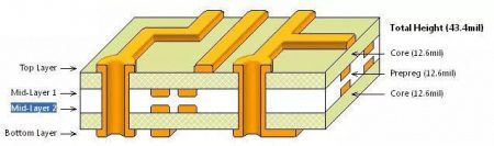
Multi-layer PCB has many advantages, such as: high assembly density, small volume; Shorten the connection between electronic components, fast signal transmission speed, convenient wiring; Good shielding, and so on. There is no limit to the number of layers of multilayer boards. There are more than 100 layers of PCBS, and four and six layers are common.
In the design of multilayer, the layers should be symmetrical, and preferably an even number of copper layers, if not symmetrical, will easily cause distortion. Multilayer board wiring is carried out according to the circuit function, in the outer wiring, the requirement is more wiring on the welding surface, less wiring on the component surface, which is conducive to the maintenance and troubleshooting of printed board.
In wiring, it is necessary to separate the power layer, the ground layer and the signal layer to reduce the interference among the power source, ground and signals. The lines of the adjacent two layers of printed boards should be perpendicular to each other as far as possible or follow oblique lines and curves, not parallel lines, in order to reduce the layer coupling and interference of the substrate.
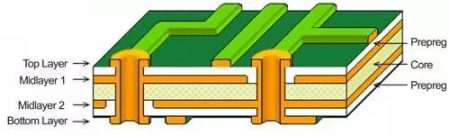
Compared with single side and double side, multi-layer PCB is composed of which layers, what each layer represents and what is its use? Multi-layer PCB’s are mainly composed of: Signal Layers, Internal Planes (internal power source), Mechanical Layers (Mechanical layer), Masks (resistance layer), Silkscreen (Silkscreen layer), and System (System working layer).
The signal layer is divided into the top layer, the middle layer and the bottom layer, which are mainly used for placing various components, or for wiring and soldering. The internal power layer, also known as the internal power layer, is used for laying out power lines and ground wires. The mechanical layer is generally used to place indicative information about the board making and assembly method, such as the physical dimension line of the circuit board, data data, through hole information, etc.
There is also a top layer and a bottom layer on which pads or other objects are placed that are copper-free areas. The screen printing layer is mainly used to draw the outline of the component, place the number of the component or other text information, and the system working layer is used to display the information that violates the design rules.


XPCB Limited is a premium PCB & PCBA manufacturer based in China.
We specialize in multilayer flexible circuits, rigid-flex PCB, HDI PCB, and Rogers PCB.
Quick-turn PCB prototyping is our specialty. Demanding project is our advantage.
Tel : +86-136-3163-3671
Fax : +86-755-2301 2705
Email : [email protected]
© 2023 - XPCB Limited All Right Reserve


