

Printed circuit board is mainly composed of bonding pad, through-hole, mounting hole, wire, components, connectors, filler, electrical boundary, etc. On printed circuit board, we will see holes that it is very porous, especially with many through-holes (vias).

There are mainly mechanical holes and laser holes on the circuit board.
Mechanical hole:
A hole drilled with a mechanical bit. The internal diameter of the hole is more than 0.2mm. The bigger the hole, the bigger the hole. Consumer electronics products are usually designed with an internal diameter of 0.3mm.
Ordinary circuit board factories can do 0.3mm mechanical holes.
If you use mechanical holes of 0.2mm and 0.25mm, the drill bit will bore slowly and break easily, which will be more expensive. Not all PCB manufacturers can make such small mechanical holes. The drill bit quickly drilled through the circuit board, so the mechanical hole is also called through hole.
Laser hole:
A hole made with a laser. The inside diameter is usually 0.1mm. There are few laser holes of other specifications. Because of the limited power of laser, it is impossible to directly punch through multi-layer PCB board, which is usually used to make blind holes in the surface layer.
With the continuous development of science and technology, there are more and more types of circuit boards. We all know that there are holes, through holes, plug-in holes, blind holes and buried holes in PCB, but there are also some special holes, such as deep control holes, countersunk holes, back holes and compression holes.
Printed circuit board control deep hole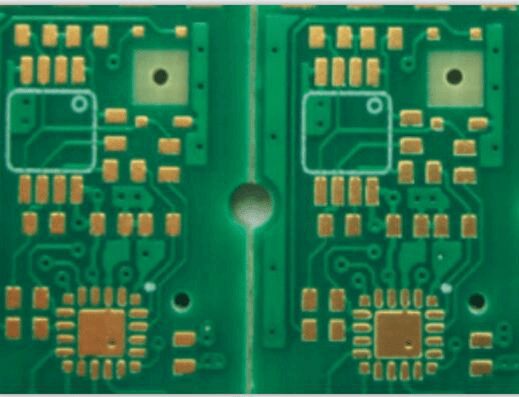
Control deep hole is not drilling through the circuit board, control a certain depth. There are many kinds of control deep hole, generally is through the mechanical drilling machine, the height of the spindle to control a certain depth of drilling. Similar mechanical blind hole, back drill, and some are deep gongs, the mechanism is the same.
Printed circuit board countersunk hole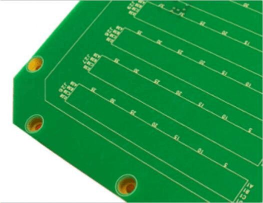
The hole in the head of the fastener or in the circuit board is called a countersunk hole. The countersunk hole of PCB board is mainly used for conduction between each layer of circuit board and fixing parts. The circuit board has very strict requirements on the depth and size of countersunk hole, and its size should be limited within the tolerance range.
Printed circuit board back drill hole
Back drilling is a kind of hole that controls the depth by mechanical drilling, removes the hole copper part of PTH hole that does not need conduction and will interfere with the signal, and retains the hole copper that needs to be used for conduction.
Design principle of back drilling hole: analyze the characteristics of signal transmission from the point of view of hole. If the design is through hole, the loop signal transmission will have to make a detour, and the existence of this section of through hole is easy to cause the reflection, scattering and other problems of signal transmission, resulting in signal disturbance and distortion.
When the extra hole copper is drilled, the signal returns according to the original way, then the inductance generated by the going signal can be offset and the distortion of the signal can be reduced to the maximum extent.
Printed Circuit board bonding hole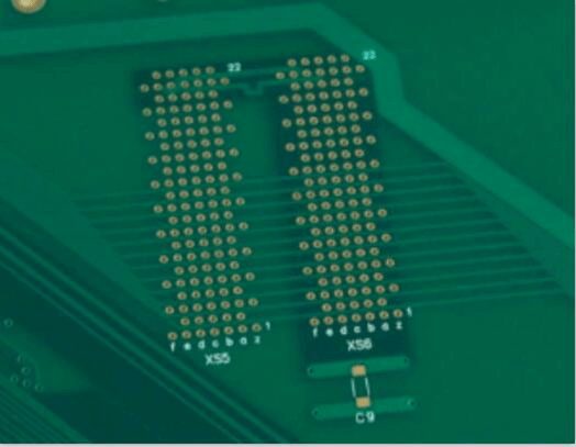
Circuit board bonding holes are those that do not require soldering and can be fixed by inserting components directly.
Its aperture tolerance is stricter than the general aperture tolerance, the conventional compression hole tolerance is +/-0.05mm, and some strict can even reach +/-0.025mm, and the need to make compression hole is mostly standard PIN components.
In the printed circuit board industry, you often hear the term half hole. Aren’t all holes drilled out round? Why only half hole?

Module PCB is basically designed with half hole, mainly for convenient welding, small module area, more functional requirements.
The usual half hole is the design hole in the single edge of the PCB, and the gong shape is cut in half, leaving only half hole in the PCB, commonly known as half hole.
The definition of metal half hole (slot) is as follows: one hole is drilled and then two holes are drilled, and the shape process ultimately retains half of the metallized hole (slot). In a simple way, the metallized hole at the edge of the plate is cut in half. The semi-metallized hole process at the edge of the plate has become a very mature process.
All metallized PCB hole positions must be drilled after drawing plating, and one hole shall be drilled at each half hole intersection point before etching.
According to years of production experience, it is suggested that designers modify the distance between the edge line and the center of the hole when designing the circuit. Generally, the center of the hole is placed on the edge line, and the control center can be moved downward. For example, the diameter of the hole is 1.4mm, the distance between the two holes is 2.54mm, the distance between the edge line of the plate is 0.33mm from the center of the through hole, and the thickness of the plate is 0.6mm.
The Angle between the cut point of the wall and the path of the milling cutter, formerly 90 degrees, is about 60 degrees this time.
Because the plate edge line from the center of the hole has a certain distance, changed the cutting Angle of the milling cutter, plus the plate thickness is particularly small, the copper hole is not easy to be pulled out.
If the design and production of small batch PCB are improved at the same time, the production yield of PCB half hole plate can be greatly improved.
PCB drilling is a process of PCB manufacturing, but also a very important step. In many cases, the multi-layer board drilling is not a finished, some holes buried in the circuit board, some on the board above through, so there will be a drill two drill.

The second hole is the hole that does not need to sink copper, such as screw hole, positioning hole, heat sink, etc., all of these holes do not need to have copper. The second drill must be behind the first drill, that is, the process is separate.
The first drill requires the process of copper sinking, that is, copper plating the hole so that it can be connected to the upper and lower layers, such as through hole, original hole and so on.
XPCB Limited is a premium PCB & PCBA manufacturer based in China.
We specialize in multilayer flexible circuits, rigid-flex PCB, HDI PCB, and Rogers PCB.
Quick-turn PCB prototyping is our specialty. Demanding project is our advantage.
Tel : +86-136-3163-3671
Fax : +86-755-2301 2705
Email : [email protected]
© 2023 - XPCB Limited All Right Reserve
