


Through the analysis of the parasitic characteristics of vias, we can see that in high-speed PCB design, seemingly simple vias often bring great negative effects to circuit design. In order to reduce the adverse effects caused by the parasitic effects of the vias, the following can be done in the design.
1. The pins of the power supply and the ground should be drilled nearby, and the lead between the via and the pin should be as short as possible, because they will increase the inductance. At the same time, the power and ground leads should be as thick as possible to reduce impedance.
2. Try not to change the layers of the signal traces on the PCB board, that is to say, try not to use unnecessary vias.
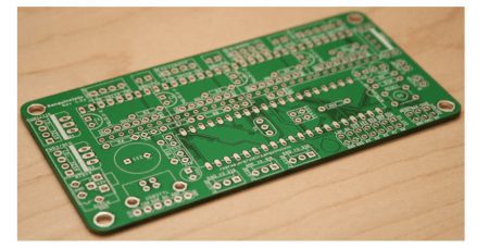
3. Considering the cost and signal quality, choose a reasonable size via size. For example, for the 6-10 layer memory module PCB design, it is better to use 10/20Mil (drilled/pad) vias. For some high-density small-size boards, you can also try to use 8/18Mil vias. Under current technical conditions, it is difficult to use smaller vias. For power or ground vias, you can consider using a larger size to reduce impedance.
4. The two formulas discussed above can be concluded that using a thinner PCB is beneficial to reduce the two parasitic parameters of the via.
5. Place some grounded vias near the vias of the signal layer to provide the nearest loop for the signal. It is even possible to place a large number of redundant ground vias on the PCB board. Of course, the design needs to be flexible. The via model discussed earlier is the case where there are pads on each layer. Sometimes, we can reduce or even remove the pads of some layers. Especially when the density of vias is very high, it may lead to the formation of a break groove that separates the loop in the copper layer. To solve this problem, in addition to moving the position of the via, we can also consider reducing the pad size of the via on the copper layer.
XPCB Limited is a manufacturer specializing in the production of high-precision double-sided, multi-layer and impedance, blind buried vias, and thick copper circuit boards. The products cover HDI, thick copper, backplanes, rigid-flex combined, buried capacitance and buried resistance, Golden Finger and other kinds of circuit boards, which can meet the needs of customers for all kinds of products.
XPCB Limited is a premium PCB & PCBA manufacturer based in China.
We specialize in multilayer flexible circuits, rigid-flex PCB, HDI PCB, and Rogers PCB.
Quick-turn PCB prototyping is our specialty. Demanding project is our advantage.
Tel : +86-136-3163-3671
Fax : +86-755-2301 2705
Email : [email protected]
© 2023 - XPCB Limited All Right Reserve
