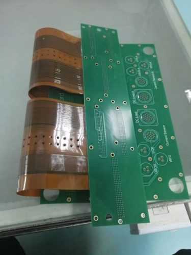
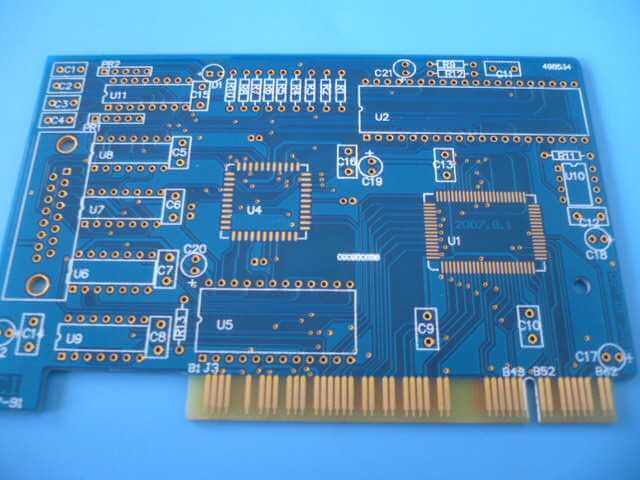
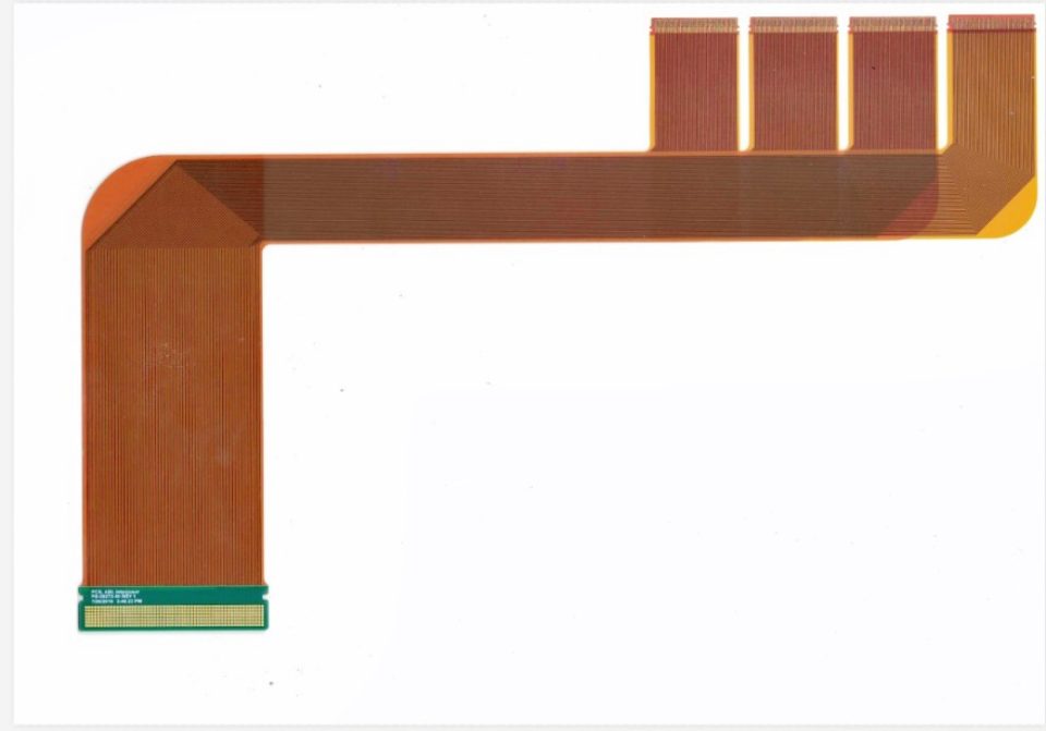
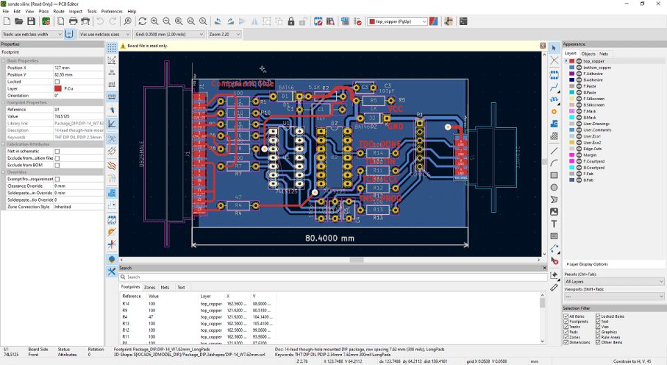







A 6-layer PCB, also known as a “multi-layer board”, is theoretically composed of three copper-clad laminates. First, the sheet metal is cut, and the inner layer of the first drilled hole is sent to the press in turn. After the 6-layer circuit board is usually pressed twice, the remanufacturing board factory will drill again, immerse copper electroplating and other processes for processing and production in turn. 6-layer printed circuit boards are relatively common in the communications industry.
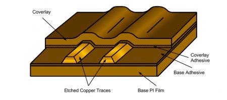
The 6-layer PCB thickness can be required to make PCB boards with different thicknesses such as 1.2mm/1.6mm/2.0mm/3.0mm. Usually different thicknesses vary from layer to layer, and the most common thickness is a 1.6mm 6-layer PCB. After PP and copper foil are fed into the press, the resin in the substrate will be dissolved and diverted by high temperature. Therefore, the pressing machine can be set to a thickness of 1.6mm, and the thickness of each layer is calculated as an average value.
Numerical calculation method of 6-layer board: Core board = 0.3mm * 2 = 0.6mm, PP = (7628 + 1080) * 4 = 0.96mm, pressed copper foil = 1OZ * 2 = 0.07mm. The theoretical value of the product is 0.6 + 0.96 + 0.07 = 1.63.
Secondly, it depends on what product the PCB is used for.
(1) Power board: If the copper thickness is too thin, it is easy to have problems in operation.
(2) Ordinary precision products: There are no special requirements for copper foil. Core board = 0.3mm * 2 = 0.6mm, PP = (7628 + 1080) * 4 = 0.96mm, pressed copper foil = 1OZ * 2 = 0.07mm.
Discover a World of Possibilities with XPCB Limited
At XPCB Limited, we’re here to help you explore new horizons. Our advanced PCB manufacturing, rapid prototyping, and turnkey PCBA solutions make it easy for you to turn your ideas into reality. Trust us to deliver excellence and reliability every step of the way. Join us and experience the power of innovation with XPCB Limited by your side.