• +86-755-23012705
  • Building 3, Jinfeng Industrial Park, Fuyong Street, Baoan District, Shenzhen ,China
  • [email protected]
logo
  • Home
  • About Us
    • Flexible PCB Expertise
    • Our Certifications
    • Our Facility
    • Quality Assurance
  • PCB Fabrication
    • Flexible PCB
    • Rigid Flex PCB
    • Rigid PCB
    • ELIC HDI PCB
    • RF PCB
    • Medical PCB
    • Automotive PCB
    • IoT & IIoT PCB
    • Industrial Control PCB
    • Telecommunication PCB
    • Consumer Electronics PCB
  • PCB Assembly
    • Turn Key PCB Assembly
    • Consigned PCB Assembly
    • Components Sourcing
  • Capabilities
    • PCB Fab Capability
    • ATE PCB Fabrication
    • PCB Technology Roadmap
    • PCB Assembly Services
    • PCB Design Support
  • Contact
  • Resources
    • PCB Blog
    • PCB Glossary
Get Quote

Is HDI Circuit Board Better Than Other PCBs?

4 layer flex circuit

4 layer Flex Circuit with HDI


What does HDI circuit board mean: HDI circuit board is HDI (high-density interconnection) PCB, which is a kind of (technology) for the production of PCBs, and a PCB with high circuit distribution density using micro-blind and buried via technology.


HDI circuit board blind and buried via PCB production process


With the development of the design of portable products in the direction of miniaturization and high density, the design of PCBs is becoming more and more difficult, which puts forward higher requirements for the PCB production process. At present, most of the portable products make the BGA package with a pitch of less than 0.65mm, and the blind and buried via design process is used, so what is the blind and buried via PCB?

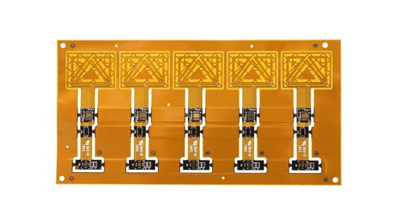
Blind and buried PCBs, also known as “HDI boards”, are often used in the application of high-end products such as mobile phones, GPS navigation, etc.

PCB holes are divided into three types: blind vias, buried vias, and through vias, among which: blind vias are the type of vias that connect the inner traces of the PCB with the traces of the surface of the PCB, and this hole does not penetrate the entire board. Buried vias are only connected to the via type of the traces between the inner layers, so they are not visible from the surface of the PCB. A through hole is a hole that can be seen directly from the top layer to the bottom layer, which is called a “through hole”. Blind and buried via PCBs


HDI circuit board manufacturer


Blind and buried via PCB

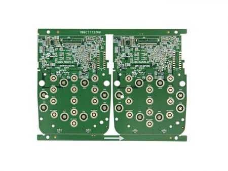
When it comes to blind/buried PCBs, the first thing that comes to mind is the high multi-layer board, which consists of an inner circuit and an outer circuit, and then uses drilling and the process of metallization in the hole to achieve the internal connection function of each layer of the circuit. However, due to the increase of line density and the continuous updating of the packaging method of the parts, in order to allow more and higher performance parts to be placed in the limited PCB area.

In addition to the finer line width, the aperture has also been reduced from 1 mm in the DIP hole diameter to 0.6 mm in the SMD, and further reduced to less than 0.4mm. However, it still occupies the surface area, so there are buried and blind vias, which are defined as follows:

  1. Buried Via: The through holes between the inner layers cannot be seen after pressing, so it does not have to occupy the area of the outer layer
  2. Blind Via is applied to the communication of the surface layer and one or more inner layers.
  3. Buried hole design and production, the production process of buried hole is more complex than that of traditional multi-layer boards, and the cost is also higher.
  4. Blind hole design and production, extremely high density, double-sided SMD design board, there will be upper and lower outer layers, I/O guide holes between each other interference, especially when there is VIP (Via-in-pad) design, it is a trouble. Blind vias can solve this problem. In addition, with the prevalence of radio communication, the design of the line must reach the range of RF (Radio frequency), more than 1GHz, and the blind via design can meet this demand.

ELIC HDI circuit board manufacturer


There are three different ways to make a blind well plate, as described below:

  1. Mechanical depth drilling, the traditional multi-layer board manufacturing process, to press, the drilling machine is used to set the Z-axis depth of drilling, but this method has several problems;
  2. Only one piece of drilling can be drilled each time, and the output is very low;
  3. The levelness of the drilling machine table is strict, and the drilling depth of each spindle should be consistent, otherwise it is difficult to control the depth of each hole;
    It is difficult to electroplating in the hole, especially if the depth is greater than the hole diameter, it is difficult to do the electroplating in the hole;


prototype HDI circuit board manufacturer


Simplify Your PCB Journey with XPCB Limited
XPCB Limited simplifies the PCB process for you. With our quick-turnaround prototyping and turnkey PCBA services, we ensure that your projects move forward smoothly and efficiently. Trust our commitment to quality and timeliness as we help you bring your designs to life. Choose XPCB Limited for a hassle-free PCB experience.


Share

Related posts

dispensing in PCB
2025-02-07

Multilayer PCB Assembly and HDI PCB Manufacturing for High-Tech Solutions


Read more
smt product line
2025-02-06

Streamline Your PCB Production with XPCB’s Turnkey PCBA Services


Read more
2025-02-05

Comprehensive Turnkey PCBA Services: From BOM to SMT Assembly


Read more
amazon
amphenol-logo
halliburton
intel logo
samtec logo
sanmina logo

Company Info

XPCB Limited is a premium PCB & PCBA manufacturer based in China.

We specialize in multilayer flexible circuits, rigid-flex PCB, HDI PCB, and Rogers PCB.

Quick-turn PCB prototyping is our specialty.  Demanding project is our advantage.

Head Office

XPCB Limited
Address :
Building 3, JinFeng Industry Area,  Fuyong Town, Baoan District, Shenzhen, Guangdong, 518103, China.

Tel : +86-136-3163-3671
Fax : +86-755-2301 2705
Email : [email protected]

Quick Links

  • Flexible PCB
  • Rigid Flex PCB
  • ELIC HDI PCB
  • RF PCB
  • PCB Capability
  • PCBA Capabiility
  • About Us

PCB Blog

Multilayer PCB Assembly and HDI PCB Manufacturing for High-Tech Solutions

Read More »

Streamline Your PCB Production with XPCB’s Turnkey PCBA Services

Read More »

Comprehensive Turnkey PCBA Services: From BOM to SMT Assembly

Read More »

© 2024 - XPCB Limited All Right Reserve