• +86-755-23012705
  • Building 3, Jinfeng Industrial Park, Fuyong Street, Baoan District, Shenzhen ,China
  • [email protected]
logo
  • Home
  • About Us
    • Flexible PCB Expertise
    • Our Certifications
    • Our Facility
    • Quality Assurance
  • PCB Fabrication
    • Flexible PCB
    • Rigid Flex PCB
    • Rigid PCB
    • ELIC HDI PCB
    • RF PCB
    • Medical PCB
    • Automotive PCB
    • IoT & IIoT PCB
    • Industrial Control PCB
    • Telecommunication PCB
    • Consumer Electronics PCB
  • PCB Assembly
    • Turn Key PCB Assembly
    • Consigned PCB Assembly
    • Components Sourcing
  • Capabilities
    • PCB Fab Capability
    • ATE PCB Fabrication
    • PCB Technology Roadmap
    • PCB Assembly Services
    • PCB Design Support
  • Contact
  • Resources
    • PCB Blog
    • PCB Glossary
Get Quote

HDI Technology and Application Introduction

HDI PCB manufacturer stackup

 HDI Circuit Board Overview & Advantages


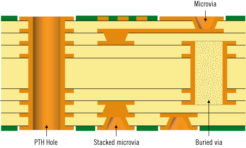
HDI circuit board refers to the microvia (Microvia) with the aperture below 6mil, the hole ring diameter (HolePad) below 0.25mm, and the contact density at 130 points/square inch Above, the wiring density is above 117 inches/square inch, and its line width/spacing is below 3mil/3mil.


Generally speaking, HDI circuit boards have the following advantages:


  1. Can reduce PCB cost: When the density of PCB increases more than eight-layer board, it is manufactured with HDI, and its cost will be lower than that of the traditional complex pressing process.
  2. Increase line density: The interconnection of traditional circuit boards and parts must be connected through the lines and through-hole conductors drawn around the QFP (fan-in and fan-out), so these lines need to occupy some space. The microvia technology can hide the wiring required for interconnection to the next layer. The bonding pads and leads between different layers are directly connected by blind holes in the pads, without fan-in and fan-out wiring. Therefore, some solder pads (such as mini-BGA or CSP small ball soldering) can be placed on the outer board surface to accept more parts and increase the density of the circuit board. At present, many mobile phone boards of high-function small wireless phones use this new stacking and wiring method.
  3. Conducive to the use of advanced assembly technology: The general traditional drilling technology cannot meet the needs of small parts of the new generation of fine lines due to the size of the pad (through hole) and mechanical drilling. With the advancement of microvia technology, designers can design the latest high-density IC packaging technologies, such as Arraypackage, CSP, and DCA (DirectChipAttach), into the system.
  4. Have better electrical performance and signal accuracy: the use of microvia interconnection can reduce signal reflection and crosstalk interference between lines, and enable the circuit board circuit design to increase more space. The nature of the physical structure is that the holes are small and short, so the effects of inductance and capacitance can be reduced, and the exchange noise during signal transmission can also be reduced.
  5. Better reliability: because of the thinner thickness and 1:1 aspect ratio of micro-holes, the reliability of signal transmission is higher than that of ordinary through holes.
  6. Improved thermal properties: The insulating dielectric material of HDI board has a higher glass transition temperature (Tg), so it has better thermal properties.
  7. It can improve radio frequency interference/electromagnetic wave interference/electrostatic discharge (RFI/EMI/ESD): the micro-hole technology allows the circuit board designer to shorten the distance between the ground layer and the signal layer to reduce radio frequency interference and electromagnetic wave interference; on the other hand, it can Increase the number of grounding wires to prevent parts in the circuit from being damaged due to instantaneous discharge caused by static electricity accumulation.
  8. Improve design efficiency: The micro-hole technology allows the circuit to be arranged in the inner layer, so that the PCB designer has more design space, so the PCB efficiency design can be higher.

RIGID FLEx PCB BLOG HDI Technology and Application Introduction


HDI Applications


HDI technology is a critical component of most of today’s innovative modern technologies. The miniaturization of digital parts consisting of PCBs has actually allowed suppliers to generate smaller sized, much more cost-efficient devices without compromising efficiency or reliability. Here are simply a few of the sectors that make use of HDI PCBs, in addition to just how they utilize them:


Consumer Electronic devices: Computers made use of to take up whole rooms, and now, thanks partly to HDI modern technology, tools as tiny as smartwatches are basically miniature desktop computers. You can find HDI boards in laptop computers, smartphones, tablets and also wearables, as well as other consumer electronics like digital video cameras as well as GENERAL PRACTITIONERS tools. HDI PCBs play a vital function in enabling the daily consumer to gain access to these powerful innovations. They’re also essential parts of IoT devices for the house, including smart thermostats, fridges as well as the many various other connected gadgets readily available. As these wise gadgets become more typical, so do HDI boards.


Communications: Along with mobile phones and laptops, HDI PCBs likewise show up in the tools that allows those tools to function, such as routers, switches, components and semiconductors. Anytime you use electronic interactions, a digital device or a tool that uses radio waves, there’s a great chance you’re using an HDI board. Digital video and also audio equipment also frequently uses HDI innovation. These boards are present in devices utilized for individual interaction, in addition to the networks used by organisations.


Automotive and also Aerospace: HDI PCBs permit suppliers to fit even more abilities right into smaller sized areas and also gadgets that consider much less. This is especially beneficial in the vehicle and also aerospace industries, where lower weight can mean much more efficient procedure. Like practically everything else, cars are becoming much more connected and computerized. Today’s autos have around 50 microprocessors on board that play a role in engine controls, diagnostics, security features and also various other benefits. Numerous new features such as onboard WiFi and GENERAL PRACTITIONERS, rearview electronic cameras as well as backup sensors count on HDI PCBs. As vehicle innovation continues to breakthrough, HDI technology will likely play a significantly important role.


Medical Industry: Advanced digital medical devices– consisting of some types of tools for monitoring, imaging, surgeries, lab analysis as well as other uses– might integrate HDI boards. The high-density innovation promotes enhanced efficiency and smaller sized, much more cost-effective devices, possibly improving the precision of surveillance as well as medical screening.


Industrial Automation: Industrial equipment is additionally becoming extra electronic, and IoT tools are becoming a lot more typical in manufacturing, warehousing and also other commercial settings. Many of this innovative tools uses HDI innovation. Today, organisations use digital tools to track supply as well as screen tools efficiency. Increasingly, machinery consists of clever sensing units that collect use information and also link to the web to interact with other wise gadgets, in addition to pass on information to administration and help optimize operations.


HDI PCB quote request HDI Technology and Application Introduction

Share

Related posts

dispensing in PCB
2025-02-07

Multilayer PCB Assembly and HDI PCB Manufacturing for High-Tech Solutions


Read more
smt product line
2025-02-06

Streamline Your PCB Production with XPCB’s Turnkey PCBA Services


Read more
2025-02-05

Comprehensive Turnkey PCBA Services: From BOM to SMT Assembly


Read more
amazon
amphenol-logo
halliburton
intel logo
samtec logo
sanmina logo

Company Info

XPCB Limited is a premium PCB & PCBA manufacturer based in China.

We specialize in multilayer flexible circuits, rigid-flex PCB, HDI PCB, and Rogers PCB.

Quick-turn PCB prototyping is our specialty.  Demanding project is our advantage.

Head Office

XPCB Limited
Address :
Building 3, JinFeng Industry Area,  Fuyong Town, Baoan District, Shenzhen, Guangdong, 518103, China.

Tel : +86-136-3163-3671
Fax : +86-755-2301 2705
Email : [email protected]

Quick Links

  • Flexible PCB
  • Rigid Flex PCB
  • ELIC HDI PCB
  • RF PCB
  • PCB Capability
  • PCBA Capabiility
  • About Us

PCB Blog

Multilayer PCB Assembly and HDI PCB Manufacturing for High-Tech Solutions

Read More »

Streamline Your PCB Production with XPCB’s Turnkey PCBA Services

Read More »

Comprehensive Turnkey PCBA Services: From BOM to SMT Assembly

Read More »

© 2024 - XPCB Limited All Right Reserve