


Bare copper plate: Pure copper is easily oxidized if exposed to the air, and the outer layer must have the above protective layer. Therefore, surface treatment is required in the circuit board processing.
OSP : OSP is different from other surface treatment processes in that it acts as a insulation layer between copper and air. Simply put, OSP is grown on a clean bare copper surface by chemical reaction. It is an organic film. Asit is organic, not metal, it is cheaper than tin spraying. Many computer motherboards use OSP technology. Because the board sizeis too large, OSP technology is more cost-saving.
1)OSP is transparent, so it is difficult to check if it is processed well.
2)OSP itself is insulated and non-conductive, which will affect electrical testing. Therefore, the test point must be opened with a stencil and printed with solder paste to remove the original OSP layer to contact the pin point for electrical testing. OSP can’t be used to handle electrical contact surfaces, such as keyboard surfaces for keys.
3)OSP is easily affected by acid and temperature. When used in the secondary reflow soldering, it needs to be completed within a certain period of time, usually the second reflow soldering effect will be relatively poor. If it is exposed to air over months, it must be resurfaced. It must be used up within 24 hours after opening the package
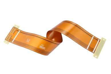
Gold-plating: Gold plating uses real gold, even if it is only plated with a thin layer, it already accounts for nearly 10% of the cost of the circuit board. The use of gold as a plating layer is one for facilitating welding and the other for preventing corrosion. Even the gold fingers of the memory sticks that have been used for several years are still shining as before. If the copper, aluminum, and iron used for the same time are used, they are now rusted into a pile of scraps. The gold-plated layer is widely used in the component pads, gold fingers, and connector shrapnel of the circuit board. The motherboards of the most widely used mobile phone circuit boards are mostly gold-plated boards, immersed gold boards, computer motherboards, audio and small digital circuit boards are generally not gold-plated boards.
Chemical gold/immersion gold: Chemical nickel immersion gold (ENIG), also known as chemical nickel gold, immersion nickel gold, referred to as chemical gold and immersion gold. ENIG is a thick nickel-gold alloy with good electrical properties on the copper surface through chemical methods and can protect PCB for a long time. The deposition thickness of the inner layer of nickel is generally 120~240μin (about 3~6μm), and the deposition thickness of the outer layer of gold is generally 2~4μinch (0.05~0.1μm). Unlike OSP, which is only used as an anti-rust layer, it can protectelectrical performance even long time use. In addition, it can endure rougher environmental change than other finish treatment methods.
1)good coplanarity, which is suitable for key contact surfaces.
2) ENIG has excellent solderability, gold will quickly melt into the molten solder, and the solder and Ni form a Ni/Sn metal compound.
Electroless nickel-palladium immersion gold: Compared with nickel-gold, ENEPIG adds a layer of palladium between nickel and gold. During the deposition reaction of replacement gold, the electroless palladium layer will protect the nickel layer from being replaced by gold. Excessive corrosion, palladium is fully prepared for immersion gold while preventing corrosion caused by substitution reaction. The deposition thickness of nickel is generally 120~240μin (about 3~6μm), and the thickness of palladium is 4~20μin (about 0.1~0.5μm). The deposition thickness of gold is generally 1~4μin (0.02~0.1μm).
HASL: HASL is also known as hot air solder leveling. It is a process of coating molten tin-lead solder on the surface of the PCB and leveling (flattening) with heated compressed air to form a layer that is resistant to copper oxidation and Can provide a coating layer with good solderability. During hot air leveling, the solder and copper form a copper-tin metal compound at the junction, and its thickness is about 1 to 2 mils.Spraying a layer of tin on the outer layer of the copper circuit can also help soldering. But it cannot provide long-term contact reliability like gold. It has no effect on the components that have been soldered, but the reliability is not enough for the pads that have been exposed to the air for a long time, such as grounding pads and pin sockets. Long-term use is prone to oxidation and corrosion, resulting in poor contact. Basically used as the circuit board of small digital products, without exception, the spray tin board, the reason is that it is cheap.
Immersion silver: The immersion silver process is between OSP and electroless nickel/immersion gold, and the process is simple and fast. Immersion silver is a displacement reaction, it is almost submicron pure silver coating (5~15μin, about 0.1~0.4μm). Sometimes the immersion silver process also contains some organic matter, mainly to prevent silver corrosion and eliminate the problem of silver migration. It is generally difficult to measure this thin layer of organic matter. Analysis shows that the weight of the organism is less than 1%. Even if exposed to heat, humidity and pollution, it can still provide good electrical properties and maintain good solderability, but it will lose gloss. Because there is no nickel under the silver layer, immersion silver does not have the good physical strength of electroless nickel/immersion gold.
Immersion Tin: Since all solders are currently tin-based, the tin layer can match any type of solder. However, tin whiskers are prone to appear in the previous PCBs after the immersion tin process, and the tin whiskers and tin migration during the soldering process will cause reliability problems, thus limiting the use of the immersion tin process. Later, organic additives were added to the tin immersion solution to make the tin layer structure a granular structure, which overcomes the previous problems, and also has good thermal stability and solderability.
Each surface treatment process has its own unique features, and the scope of application is also different. However, ENEPIG is a universal processing method that can meet the requirements of various assembly occasions.
XPCB Limited is a premium PCB & PCBA manufacturer based in China.
We specialize in multilayer flexible circuits, rigid-flex PCB, HDI PCB, and Rogers PCB.
Quick-turn PCB prototyping is our specialty. Demanding project is our advantage.
Tel : +86-136-3163-3671
Fax : +86-755-2301 2705
Email : [email protected]
© 2023 - XPCB Limited All Right Reserve
