


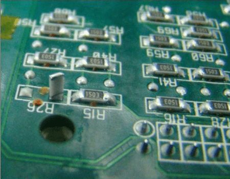
In the PCBA processing industry in Shenzhen, most PCBA manufacturers will encounter an undesirable phenomenon. One end of the chip component will lift up during SMT. This situation mostly occurs in small-size chip resistor-capacitor components, especially 0402 chip capacitors and chip resistors. This phenomenon is often referred to as the “tombstone phenomenon”.
Causes:
(1) The melting time of the solder paste at both ends of the components is not synchronous or the surface tension is different, such as poor solder paste printing (one end is incomplete), offset sticking, and different sizes of the welding ends of the components. Generally, the melted end of the solder paste is pulled up.
(2) Pad Design: There must be a suitable range for the elongation of the pad. Tombstone phenomenon is easy to occur if it is too short or too long.
(3) If the solder paste is too thick, the components will float up after the solder paste melts. In this case, the components are easy to be erected due to hot wind blowing.
(4) Temperature Curve Setting: The tombstone generally occurs at the moment when the solder joints begin to melt. The heating rate near the melting point is very important. The slower it is, the better it is to eliminate the tombstone phenomenon.
(5) One welding end of components is oxidized or contaminated and cannot be wetted. Special attention shall be paid to components with single-layer silver welding end.
(6) The pad is contaminated (with silk screen, solder resist ink, foreign matters adhered and oxidized).
Mechanism of Formation:
During reflow soldering, the upper and lower surfaces of the chip components are heated at the same time. Generally speaking, the pad with the largest exposed area is first heated to a temperature above the melting point of the solder paste. In this way, one end of the component wetted by the solder is often pulled up by the surface tension of the solder at the other end.
Solution:
(1) Design
Properly design the pad-the extension size must be reasonable, and try to avoid the situation where the wetting angle of the outer edge (straight line) of the pad formed by the extension length is greater than 45°.
(2) Production Site
(3) Incoming Materials
Strictly control the quality of incoming materials to ensure that the effective area of the two ends of the components used is the same (the basis for surface tension).
Our company XPCB Limited has been professional PCBA processing in Shenzhen for nearly 20 years, has a large number of advanced technology and engineers, has rich experience in dealing with various types of PCBA processing defects, and look forward to cooperating with you!
XPCB Limited is a premium PCB & PCBA manufacturer based in China.
We specialize in multilayer flexible circuits, rigid-flex PCB, HDI PCB, and Rogers PCB.
Quick-turn PCB prototyping is our specialty. Demanding project is our advantage.
Tel : +86-136-3163-3671
Fax : +86-755-2301 2705
Email : [email protected]
© 2023 - XPCB Limited All Right Reserve
