• +86-755-23012705
  • [email protected]
  • Building 3, Jinfeng Industrial Park, Fuyong Street, Baoan District, Shenzhen ,China
Search
Close
logo
  • Home
  • About Us
    • About XPCB
    • Flexible PCB Fabrication
    • PCB Fab Capability
    • PCBA Capability
    • Our Certifications
    • Our Facility
    • Quality Assurance
  • PCB Fabrication
    • Flexible PCB
    • Rigid Flex PCB
    • Rigid PCB
    • ELIC HDI PCB
    • RF PCB
    • Medical PCB
    • Automotive PCB
    • IoT & IIoT PCB
    • Industrial Control PCB
    • Telecommunication PCB
    • Consumer Electronics PCB
  • PCB Assembly
    • Turn Key PCB Assembly
    • Consigned PCB Assembly
    • Components Sourcing
  • Resources
    • PCB Glossary
    • PCB Design Guide
    • PCB Blog
  • Contact
Menu
  • Home
  • About Us
    • About XPCB
    • Flexible PCB Fabrication
    • PCB Fab Capability
    • PCBA Capability
    • Our Certifications
    • Our Facility
    • Quality Assurance
  • PCB Fabrication
    • Flexible PCB
    • Rigid Flex PCB
    • Rigid PCB
    • ELIC HDI PCB
    • RF PCB
    • Medical PCB
    • Automotive PCB
    • IoT & IIoT PCB
    • Industrial Control PCB
    • Telecommunication PCB
    • Consumer Electronics PCB
  • PCB Assembly
    • Turn Key PCB Assembly
    • Consigned PCB Assembly
    • Components Sourcing
  • Resources
    • PCB Glossary
    • PCB Design Guide
    • PCB Blog
  • Contact
Get Instant Quote

How To Design 4 Layer Flexible PCB(FPC)? 3 Solutions Inside


When designing a 4 layer flexible PCB, how is the stackup generally designed?


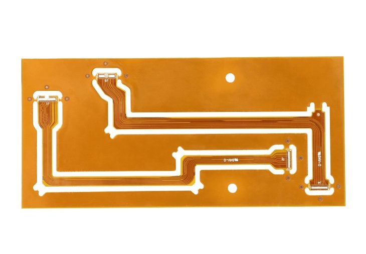
In theory, there can be three options.


Option I

1 power layer, 1 ground layer and 2 signal layers are arranged in this way: TOP (signal layer), L2 (ground layer), L3 (power layer), BOT (signal layer).

Option II

One power layer, one ground layer and two signal layers are arranged in this way: TOP (power layer), L2 (signal layer), L3 (signal layer), BOT (ground layer).

Option III

1 power layer, 1 ground layer and 2 signal layers are arranged in this way: TOP (signal layer), L2 (power layer), L3 (ground layer), BOT (signal layer).


flex pcb board printing48205627235 How To Design 4 Layer Flexible PCB(FPC)? 3 Solutions Inside


Question follow above suggestions is what are the pros and cons of these three options? You can check below detailed explaination. 


Option I

The main laminated design scheme of the 4 layer flexible PCB has a ground plane under the component surface, and the key signal is preferably placed on the TOP layer; as for the layer thickness setting, the following suggestions are made: the impedance control core board (GND to POWER) should not be too thick so as to reduce the distributed impedance of the power supply and ground plane; ensure the decoupling effect of the power plane.


Option II

These solutions are mainly to achieve a certain shielding effect, placing the power supply and ground plane on the TOP and BOTTOM layer. While following defects may occur if hoping to get perfect shielding effect by this solution.

  1. The power and ground are too far apart, and the power plane impedance is large.
  2. The power supply and ground plane are extremely incomplete due to the influence of component pads. Because the reference plane is incomplete and the signal impedance is not continuous, in fact, due to the large number of surface mount devices, the power supply and ground of this solution can hardly be used as a complete reference plane, and the expected shielding effect is very Difficult to achieve;

Solution 2 has a limited range of use. But in individual boards, Solution 2 is the best layer setting solution.


 Option III

This scheme is similar to scheme 1, and is suitable for the case where the main components are laid out in the BOTTOM layout or the bottom layer of key signals.

Share

Related posts

2022-05-20

Electromagnetic Compatibility Design of Mobile Phone PCB (1)


Read more
2022-05-20

The PCB Circuit Design of LED Switching Power Supply


Read more
2022-05-20

Electromagnetic Compatibility Design of Mobile Phone PCB (2)


Read more
amazon
amphenol-logo
halliburton
intel logo
samtec logo
sanmina logo
Previous
Next

Company Info

XPCB Limited is a premium PCB & PCBA manufacturer based in China.

We specialize in multilayer flexible circuits, rigid-flex PCB, HDI PCB, and Rogers PCB.

Quick-turn PCB prototyping is our specialty.  Demanding project is our advantage.

Head Office

XPCB Limited
Address :
Building 3, JinFeng Industry Area,  Fuyong Town, Baoan District, Shenzhen, Guangdong, 518103, China.

Tel : +86-136-3163-3671
Fax : +86-755-2301 2705
Email : [email protected]

Quick Links

  • Flexible PCB
  • Rigid Flex PCB
  • ELIC HDI PCB
  • RF PCB
  • PCB Capability
  • PCBA Capabiility
  • About Us

PCB Blog

Electromagnetic Compatibility Design of Mobile Phone PCB (1)

Read More »

The PCB Circuit Design of LED Switching Power Supply

Read More »

Electromagnetic Compatibility Design of Mobile Phone PCB (2)

Read More »

© 2023 - XPCB Limited All Right Reserve