How to design a multilayer PCB board?
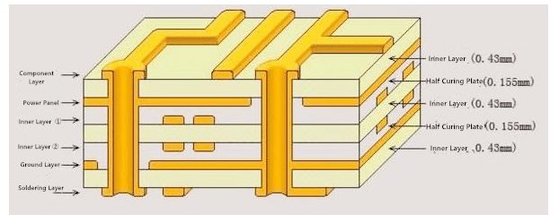
Multi-layer printed circuit board design technology is similar to double-sided PCB design, and the wiring is easier. First of all, you have to divide the layered structure. For easier designing, it is best to use the substrate as the center, symmetrically distributed to both sides, and the adjacent signal layers are electrically grounded. Secondly, ask the PCB manufacturer for the parameters (dielectric constant, line width, curium thickness, board thickness) for impedance matching. These parameters do not need to be calculated by themselves and should be provided by the PCB manufacturer. With these parameters, you can calculate the line width, line spacing, and line length, and then you can start PCB drawing. There are three types of hole connected multi-layer boards: blind holes, buried holes, and vias, which makes wiring job easily, but these connection methods are expensive. The high-speed line is best to place in the inner layer because the top and bottom layers are easily affected by outside temperature, humidity, and air. If you need to test, you can make a test via.
What are the advantages of multilayer PCB? Although single-layer circuit boards have their advantages, multi-layer designs are more advantageous for certain applications. If you want to know the advantages of multilayer PCB, you must understand what multilayer PCB is beforehand. Check it here. For some devices, it is necessary to use a multilayer PCB to meet the requirements. What are the benefits of more complex multilayer PCBs?
- Useful for more complex projects: devices that are more complex and involve more circuits and components usually require the use of multilayer PCBs. If it requires more circuits than can fit on a single circuit board, you can add space by adding layers. Having multiple circuit boards ensures enough connection space, making it ideal for more advanced equipment. Devices with many different uses and advanced features, such as smartphones, require this level of complexity.
- High quality: Multilayer circuit boards require more planning and intensive production processes, so they usually have higher quality than other types of printed circuit boards. The design and production of these circuit boards require more skills and more advanced tools than simple components, thereby increasing the possibility of obtaining high-quality products. Many of these designs include advanced controlled impedance characteristics and electromagnetic interference shielding to further improve performance.
- Increased power: Due to the increased circuit density of multilayer PCBs, they are more powerful than less complex designs. They have a higher operating capacity and can run at higher speeds, which are usually necessary for the advanced equipment they power and can improve performance.
- Improve durability and therefore more durable than single-sided PCB. This is another reason why adding functionality through additional layers is better than increasing the size of a single layer. This enhanced durability means that circuit boards can withstand harsher conditions and can generally last longer.
- The smaller size and lighter weight: Multi-layer PCBs achieve this enhanced durability while still maintaining a relatively small size and lighter weight. Because they will be layered together, so you space. This smaller size also means lighter weight. Single-layer boards match it with multiple single-layer boards, but this also increases the size and weight of the final product.
- Single connection point: The use of multiple PCB components requires multiple connection points. On the other hand, multi-layer boards are designed to work with a single connection point, simplifying the design of electronic devices and further reducing weight. When deciding whether to use multiple single panels instead of just one multilayer printed circuit board, multilayer boards are usually the best choice.


