- +86-755-23012705
- Building 3, Jinfeng Industrial Park, Fuyong Street, Baoan District, Shenzhen ,China
- [email protected]
Everybody knows that impedance has to be continuous.

There are always times when the impedance of a PCB design is not continuous. How to do?
Characteristic impedance: also known as “characteristic impedance”, it is not a DC resistance and belongs to the concept of long line transmission. In the high-frequency range, a transient current is generated between the signal line and the reference plane (power source or ground plane) along with the arrival point of the signal during signal transmission due to the establishment of an electric field.
If the transmission line is isotropic, there will always be current I as long as the signal is being transmitted. If the output voltage of the signal is V, the transmission line will be equivalent to a resistance of V/I during the signal transmission. This equivalent resistance is called the characteristic impedance Z of the transmission line.
During the transmission of a signal, if the characteristic impedance along with the transmission path changes, the signal will be reflected at the node where the impedance is discontinuous. The factors affecting characteristic impedance are dielectric constant, dielectric thickness, line width, and copper foil thickness.
[1] Gradient line

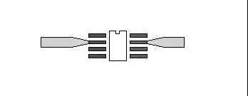
Some RF devices have small packages. SMD pads may be as small as 12mils in width, while RF signal lines may be more than 50mils in width. Gradient lines should be used, and abrupt changes in line width are prohibited. The gradient line is shown in the figure. The transition line should not be too long.
[2] Corner

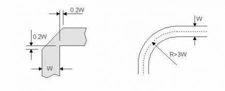
If the RF signal line takes a right angle, the effective linewidth at the corner will increase, and the impedance will be discontinuous, causing the signal reflection. To reduce discontinuity, there are two ways to treat corners: cut corners and rounded corners. The radius of the arc Angle should be large enough, in general, to ensure: R>3 w. This is shown on the right.
[3] Large welding pad

When there is a large pad on the 50-ohm stripline, the large pad ACTS as a distributed capacitance and destroys the characteristic impedance continuity of the stripline. Two methods can be adopted simultaneously to improve: firstly, thickening the micro-strip line medium and secondly, hollowing out the ground plane below the pad can reduce the distributed capacitance of the pad. The diagram below.
[4] Through the hole

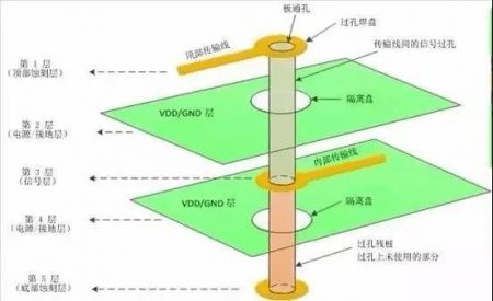
The through-hole is a metal cylinder outside the through-hole between the top and bottom layers of the circuit board. The signal passes through the hole to connect the transmission line on different layers. The through-hole stump is the unused part of the through-hole. The through-hole pads are circular gaskets that connect the through-hole to the top or internal transmission lines. The isolation panel is a circular void within each power supply or connection to prevent short circuits from reaching the power supply and connection.
Parasitic parameters through the hole
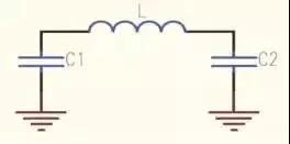
After strict physical theory deduction and approximate analysis, the equivalent circuit model of the through-hole can be described as a grounding capacitor at each end of an inductor in series, as shown in the picture.

Equivalent circuit model of through-hole
Based on the equivalent circuit model, it can be seen that there is parasitic capacitance through the hole itself. Assuming that the diameter of the through-hole back solder pad is D2, the diameter of the through-hole back solder pad is D1, the thickness of the PCB board is T, and the dielectric constant of the pad substrate is, the parasitic capacitance through the hole is approximate:
The parasitic capacitance through the hole can cause the signal rising time to be prolonged and the transmission speed to be slowed down, thus worsening the signal quality.
Similarly, there is also parasitic inductance through the hole. In high-speed digital PCB, the hazard of parasitic inductance is often greater than that of parasitic capacitance.
Its parasitic series inductance will weaken the contribution of bypass capacitance, thus weakening the filtering effect of the whole power supply system.
Suppose L is the inductance through the hole, H is the length through the hole, and D is the diameter of the central hole.
Through-hole is one of the important factors causing impedance discontinuity on RF channel. If the signal frequency is more than 1GHz, the influence of through-hole should be considered.
The common methods to reduce the discontinuity of impedance through-hole include: adopting disk less process, selecting outlet mode, optimizing the diameter of the back welding pad, etc. Optimizing the diameter of the back welding pad is one of the most commonly used methods to reduce impedance discontinuities. Since the through-hole characteristics are related to the size of the pore size, welding pad, back welding pad, cascade structure, outlet mode, and other structures, it is suggested that HFSS and Optimetrics should be used for optimization simulation in each design according to the specific situation.
When parameterized models are used, the modeling process is simple. During the review, the PCB designer is required to provide the corresponding simulation documentation.
The diameter of the holes, the diameter of the pads, the depth of the pads, and the back pads can all change, causing impedance discontinuities, and the severity of the reflection and insertion losses.
[5] Through-hole coaxial connector
Similar to the through-hole structure, the through-hole coaxial connector also has impedance discontinuity, so the solution is the same as the through-hole. The common methods to reduce impedance discontinuities of through-hole coaxial connectors are also as follows: adopting diskless technology, appropriate outlet mode, and optimizing the diameter of the back welding pad.


XPCB Limited is a premium PCB & PCBA manufacturer based in China.
We specialize in multilayer flexible circuits, rigid-flex PCB, HDI PCB, and Rogers PCB.
Quick-turn PCB prototyping is our specialty. Demanding project is our advantage.
Tel : +86-136-3163-3671
Fax : +86-755-2301 2705
Email : [email protected]
© 2024 - XPCB Limited All Right Reserve
